1.4. Error display
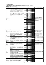
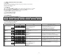
See the table below for descriptions of displayed errors and countermeasures for these.
Display order is
q
,
w
,
e
,
r
,
t
,
y
,
u
.
Condition
States
Display
TROUBLE SHOOTING
q
Firm Check
NG
The model name, brand name and region infor-
mation written in the firmware are compared
to the region settings in the PCB.This error is
displayed if the information does not match.
" ▲ " or " ▼ " is displayed as the first character if
the firmware is not correct (see right section of
table).
FLD
L1
F I R M
L2
E R R O R
L3
FLD
L1
M A I N
–
L2
* * * * * * * *
L3
B
L - * * . *
*
FLD
L1
S U B
–
L2
X X Y Z * * * *
L3
B
L - * * . *
*
FLD
L1
D S P
–
L2
L3
* * . *
*
FLD
L1
A . P L
D
–
L2
L3
* * . *
*
FLD
L1
G U I
–
L2
L3
* * . *
*
• Check the resistor for set-
ting region(R1428 / R1431,
HDMIPCB).
• Write the firmware for the
correct region.
w
SUB μ -COM
NG
There is not a reply from SUBμ-COM.
FLD
L1
E 2 P R
O M
L2
E R R O R
L3
* * *
• Check the SUB(U1020) and
surrounding circuits.
e
IP SCALER NG
An error occurs in Loopback Test of the DDR
memory to perform at initial setting of i/p
Scaler(ADV8003).
FLD
L1
I P
L2
S C A L E R
L3
E R R
0 1
• Check the circuits around
the IP SCALER (U1026,
HDMI PCB) and DDR2
(U1028/1029).
If there appear to be no prob-
lems, U1026 or U1028/1029 is
faulty.
In initial setting of i/p Scaler ( ADV8003 ) , there
is not the reply of the Loopback Test result of
the DDR memory .
FLD L3
E R R
0 2
r
GUI Serial
Flash NG
When it is different from Version of the Main
CPU which Version of GUI Serial Flash supports .
(ADV8003)
FLD
L1
G U I
V E
R .
L2
E R R O R
L3
• Check the firmware version.
t
DIR NG
This error is displayed if there is no response
from the DIR.
FLD
L1
D I R
L2
E R R O R
L3
0 1
• Check the DIR (U1040, HDMI
PCB) and surrounding cir-
cuits.
y
DSP NG
The DSP FLAG0 port does not enter "
Hi
" status
even after executing a DSP reset during a DSP
code boot.
FLD
L1
D S P
L2
E R R O R
L3
0 1
• Check the DSP (U1024, HDMI
PCB) and surrounding cir-
cuits.
The DSP FLAG0 port does not enter "
Hi
" status
before issuing a DSP command.
FLD L3
0 2
ACK="
Hi
" does not occur during DSP data read-
ing, even when WRITE="
Lo
".
FLD L3
0 3
ACK="
Lo
" does not occur during DSP data read-
ing, even when REQ="
Lo
".
FLD L3
0 4
ACK="
Hi
" does not occur during DSP data writ-
ing, even when WRITE="
Hi
".
FLD L3
0 5
ACK="
Lo
" does not occur during DSP data writ-
ing, even when REQ="
Lo
".
FLD L3
0 6
u
EEPROM NG
An error occurred in a checksum of the EE-
PROM(*** is a block address number).
FLD
L1
E 2 P R
O M
L2
E R R O R
L3
* * *
21


