Section 13: Microprocessor Computer and Control –Theory of Operation
13-18
Both read and write transfers between the 386EX and the 1351FLB are defined
in the 1351FLB manual, pages 1-33 and 1-34. The timing specifications of the
1351FLB for reading and writing data to and from the control registers or
display RAM, allow a direct interface to the 386EX. External control circuits in
the FPGA are not necessary, except for one signal, the READY# signal. This is
explained in a following section.
13.10.2 LCD Display RAM
The interface signals for the display RAM are prefaced with the letter V, which
indicates video RAM. The interface to the display RAM (VRAM) is defined in
the 1351FLB manual and is connected directly to the RAM.
The LCD display interfaces directly with the 1351FLB. Timing diagrams are in
the associated manuals. The signals used are LCDENB, XSCL, LP, WF, YD,
UD0-UD3, and LD0-LD3. The UD and LD signals are data lines to the upper
and lower display panels. The XSCL
is the data shift clock and the LCD display
stores the data on the falling edge of this clock. The LP
signal is the latch pulse
and is used to latch the data into the X-drivers. The YD
signal is the frame
pulse, which indicates a start-of-frame.
13.10.3 LCD FPGA Control Circuits
The LCD display chip interfaces directly with the 386EX. The only circuit that
is necessary to generate in the FPGA is the READY# circuit. The 1351
generates a wait signal when transfers are initiated . This wait signal is gated
with the LCD select signals and implements an external READY signal when the
1351 has completed the transfer.
13.11 Real-time Clock (RTC)
The RTC is a Dallas DS1693, which has the crystal and battery imbedded in the
unit. It is a 28-pin DIP package and runs from a 3.3 volts supply.
CS3# is assigned to the RTC in the I/O space and the software must assign
14 wait states to this unit.
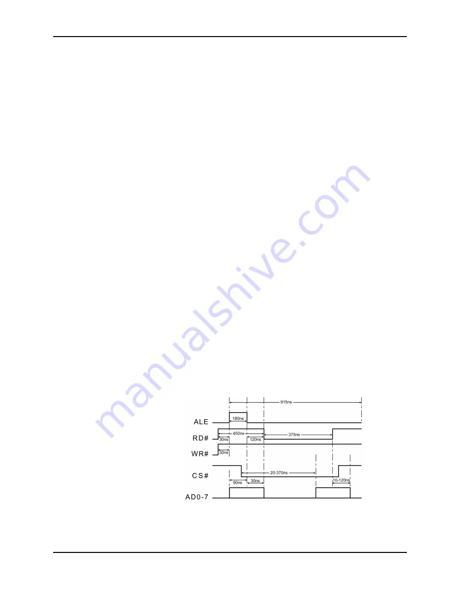
The timing for the DS1693 is shown in Figure 13-12.
Figure 13-12: DS1693 Timing
See Figure 13-13. The timing for this interface is done in the FPGA. There is a
state machine that is clocked at 20 MHz and generates 18 states.
Summary of Contents for NELLCOR NPB-4000
Page 66: ... THIS PAGE INTENTIONALLY LEFT BLANK ...
Page 68: ...Section 7 Spare Parts 7 2 Figure 7 1 NPB 4000 C Top Assembly Drawing ...
Page 70: ...Section 7 Spare Parts 7 4 Figure 7 2 NPB 4000 C Front Case Assembly Diagram Sheet 1 of 2 ...
Page 72: ...Section 7 Spare Parts 7 6 Figure 7 3 NPB 4000 C Front Case Assembly Diagram Sheet 2 of 2 ...
Page 74: ...Section 7 Spare Parts 7 8 Figure 7 4 NPB 4000 C Rear Case Assembly Diagram Sheet 1 of 2 ...
Page 76: ...Section 7 Spare Parts 7 10 Figure 7 5 NPB 4000 C Rear Case Assembly Diagram Sheet 2 of 2 ...
Page 78: ...Section 7 Spare Parts 7 12 Figure 7 6 NPB 4000 C Power Supply Heat Sink Assembly Diagram ...
Page 80: ... THIS PAGE INTENTIONALLY LEFT BLANK ...
Page 96: ... THIS PAGE INTENTIONALLY LEFT BLANK ...
Page 114: ... THIS PAGE INTENTIONALLY LEFT BLANK ...
Page 140: ... THIS PAGE INTENTIONALLY LEFT BLANK ...
Page 180: ... THIS PAGE INTENTIONALLY LEFT BLANK ...
Page 192: ... THIS PAGE INTENTIONALLY LEFT BLANK ...
Page 208: ... THIS PAGE INTENTIONALLY LEFT BLANK ...
Page 210: ... THIS PAGE INTENTIONALLY LEFT BLANK ...
Page 211: ...Section 17 Drawings 17 3 Figure 17 1 MP 205 PCB Schematic Sheet 1 of 2 ...
Page 212: ...Section 17 Drawings 17 5 Figure 17 2 MP 205 PCB Schematic Sheet 2 of 2 ...