PLL Modes
2-5
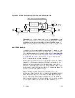
Figure 2.3
Phase and Frequency Detection with an External VCO
Prescalers (CNT_I) and a divider (CNT_O) in the feedback loop of the
PLL generate the internal operating clock (OCLK). Program the 15-bit
prescalers through the microprocessor interface, selecting values for
CNT_I and CNT_O that minimize CNT_O and reach the required ratio.
2.2.2 PLL Mode 2
In Mode 2, the PCLK input provides an external clock. The L64777 uses
the internal NCO to lock to the transport byte clock, provided at ICLK.
The chip generates an OCLK internally. Select PCLK to be at least twice
the frequency of the internal OCLK.
Appendix B, PLL Divider Settings
, describes the connection between the
L64777 and the L64724 in Mode 2 operation.
Consecutive sync blocks can have any gap length between them. Thus,
the L64777 can convert an input block to a block with a gap for RS
insertion, as long as the size of the 128-byte circular input buffer is
sufficient to insert RS gaps and to cope with possible PLL jitter. For an
encoder with 16-parity RS insertion, the L64777 selects the size of the
circular input buffer with sufficient margin.
When operating on public synchronous networks (such as the
synchronous digital hierarchy, SDH, or plesiochronous digital hierarchy,
PDH), the system designer must consider possible jitter on the input
network. The design of the L64777 permits short-term deviations of
input-to-output frequency of
±
56 bytes before a FIFO overrun condition
occurs. This is sufficient for operations on SDH or PDH networks.
OCLK
ICLK
+Z
−
current
Load
Value
Load
Value
CNT_O
CNT_I
Frequency Detect
Phase Detect
FREQ_PHASE_COMP (From Microprocessor)
2
2
From VCO
To VCO
PLL_CS
%2
%2
Summary of Contents for L64777
Page 1: ...L64777 DVB QAM Modulator Order Number I14031 A Technical Manual June 2000...
Page 10: ...x Contents...
Page 14: ...1 4 Introduction...
Page 90: ...5 10 Signals...
Page 110: ...A 8 Programming the L64777 in Serial Host Interface Mode...
Page 116: ...C 2 Monitoring Device Internal Signals...
Page 124: ......

