background image

Chapter 8 Option Boards and Memory Module 

XBC E-Type Main Unit 

8-8 

Ver. 1 


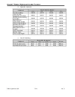
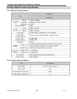
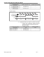
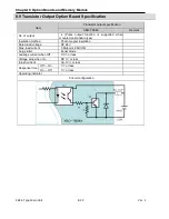
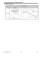
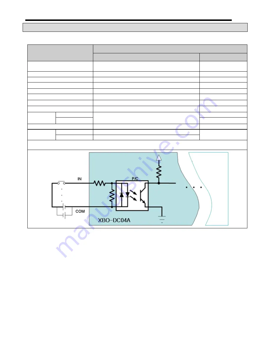
8.5 DC Input Option Board Specification 

Specification of XGB input option board is as follows. 

Item 

DC input specification 

XBO-DC04A 

Remark 

Input point  

4 points (supports high-speed counter function when 
installed at standard type) 


Insulation Method 

Photo coupler insulation 


Rated input voltage 

DC24V 


Rated input current 

About 10


Voltage range 

DC20.4~28.8V (ripple rate within 5%) 


On voltage / On current 

DC19V or above / 3

 or above 


Off voltage / Off current 

DC6V or less / 1

 or less 


Input resistance 

About 2.7


Response 
time 

Off → On 

1/3/5/10/20/70/100

  (set through I/O  parameter) 

Initial value: 3


On → Off 


Common method 

4 points / COM 

″ 

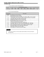
High speed 
counter 

Performance 

4kpps 4 channels (based on 1 phase) 

when installed at 
standard type 

Mode 

Linear counter 

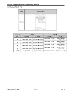
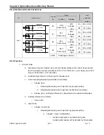
Circuit configuration 


Standard/ 

economic type 

Summary of Contents for XBC-DN10E

Page 1: ......

Page 2: ...s violated This symbol indicates the possibility of slight injury or damage to products if applicable instruction is violated This symbol indicates dangerous voltage present Electrical shock hazard is...

Page 3: ...DP30SU XBC DP40SU XBC DP60SU 2 Data Backup time modified 4 14 V1 6 2014 09 1 Domain of Homepage changed 2 RTC Option specification added Available on slot 9 Front Back Cover 2 2 2 4 9 4 V1 7 2015 02 2...

Page 4: ...our website http www lsis com and download the information as a PDF file Relevant User s Manual Title Description No of User Manual XG5000 User s Manual Describes how to use XG5000 software and onlin...

Page 5: ...ION UNIT MM 10 3 5 PLC MOUNTING 11 3 6 WIRING GUIDELINES 15 3 6 1 Wiring General Specifications 16 3 6 2 On Board Power Supply 16 3 6 3 A C Power Input 18 3 6 4 I O Device Wiring Concepts 18 3 6 5 Dig...

Page 6: ...TA TYPES AND APPLICATION METHODS 13 4 6 1 Data types 13 4 6 2 Bit data Bit 13 4 6 3 Nibble Byte data Nibble Byte 14 4 6 4 Word data Word 15 4 6 5 Double word data DWORD 16 4 6 6 Real data REAL LREAL 1...

Page 7: ...6 3 13 Data table process instruction 22 6 3 14 Display instruction 22 6 3 15 String Process instruction 23 6 3 16 Special function instruction 25 6 3 17 Data control instruction 26 6 3 18 Time relate...

Page 8: ...RUCTIONS 280 6 38 DIVERGENCE INSTRUCTION 286 6 39 LOOP INSTRUCTION 288 6 40 FLAG INSTRUCTION 290 6 41 SYSTEM INSTRUCTION 292 6 42 INTERRUPT RELATED INSTRUCTION 300 6 43 SIGN REVERSE INSTRUCTION 302 6...

Page 9: ...Procedures 4 10 2 4 Troubleshooting Flowcharts 5 10 4 TROUBLESHOOTING EXAMPLES 11 10 4 1 Input circuit troubles and corrective actions 11 10 4 2 Output circuit and corrective actions 12 10 5 ERROR COD...

Page 10: ...Table of Contents Table of Contents 6 10 10 CLEAR ALL PLC 29...

Page 11: ...ions Wiring Guidelines and I O Schematics Chapter 4 CPU Specifications Scan Time Program Execution Memory Mapping and Environmental Specifications Chapter 5 Programming Concepts Program Execution CPU...

Page 12: ...ype XBC Dx14E XBC Dx20E 135 90 64 XBC Dx30E Extension module XBE XBF XBL 20 90 60 Basis of minimum size 3 Improved programming ability with multiple kinds of register RTC option module comment backup...

Page 13: ...base b With analog dedicated register U and monitoring dedicated function convenient use for I O is maximized can designate operations using easy programming of U area and monitoring function 7 Integr...

Page 14: ...nsion modules Option Module E type Max 2 If using 10 14 points models only one is available Items Main Unit E type XBC DR10 14 20 30E XBC DN10 14 20 30E XBC DP10 14 20 30E Item Description Items Optio...

Page 15: ...24V input 8 point transistor output 6 point XBC DP20E AC100 220V power supply DC 24V input 12 point transistor output 8 point XBC DP30E AC100 220V power supply DC 24V input 18 point transistor output...

Page 16: ...pansion unit PLC System A system which consists of the PLC and peripheral devices A user program can control the system XG5000 A program and debugging tool for the MASTER K series It executes program...

Page 17: ...l to the switch after an input signal turns on Input Sensing PLC Module Input Circuit Power Supply Common Current Optical Isolation Input Sensing Switch Sink Output Current flows from the load to the...

Page 18: ...st switch 4 A test lamp of same voltage as power supply 120V in this example 5 Small Philips or Flat screwdriver 6 A PMC 310S LSIS PLC serial programming cable 2 2 XG5000 2 2 1 Install XG5000 1 Once y...

Page 19: ...a Ladder Logic Program 1 Select the Normally Open Contact by clicking the icon in the top right of the XG5000 window and click the first cell in the first rung of the NewProgram Window to place the c...

Page 20: ...put P00 for the Variable Device and click OK to insert the contact 4 Next select the Coil by clicking the icon or pressing F9 Pressing F9 will automatically insert the coil in the last slot of the run...

Page 21: ...ype Main Unit 2 4 Ver 1 6 Input P40 for the Variable Device and click OK to insert the coil 7 You have now written a simple Ladder Logic Program This program will instruct the PLC to turn on the P40 o...

Page 22: ...1 The program can be simulated using XG5000 without needing to connect to a physical PLC 2 To start the simulator click either the taskbar icon shown below or Tools Start Simulator 3 This will open b...

Page 23: ...E Type Main Unit 2 6 Ver 1 4 The simulator allows you to control and test all functions of your ladder program Double click the P00 contact to open the Change Value window 5 Click OK to activate P00...

Page 24: ...am using PLC hardware a Connect power and I O wiring to PLC according to the drawing below b The Test Switch will be wired to input P00 using power from the on board 24VDC supply c The Test Lamp will...

Page 25: ...r 1 e Next connect the PLC to your computer using the Comm 1 port and cable 2 5 Writing Program to PLC 1 Return to XG5000 and the test program we have written 2 Open the connection settings by clickin...

Page 26: ...indow Since we are using an E type PLC in this example set Type to RS232C and Depth to Local XG5000 software will automatically detect the PC port where the PLC is connected 4 Then click Connect and O...

Page 27: ...n Unit 2 10 Ver 1 6 Since the PLC was not running when we wrote the program to it XG5000 will prompt to reset the PLC Click OK 7 To reconnect with the PLC click Online Connect 8 To run the PLC with it...

Page 28: ...Chapter 2 Quick Start Guide XBC E Type Main Unit 2 11 Ver 1 9 You can now test the program by closing the switch connected to P00 which will cause output P40 to turn on...

Page 29: ...h as resistive and inductive loads from OFF to ON momentary high inrush current up to 10 times the steady state current can occur Use an interposing relay between the module output and the controlled...

Page 30: ...be turned off and stopped for system safety However i f CPU error is caused on output device itself such as relay or TR it cannot be detected The output may be kept on which may cause s erious problem...

Page 31: ...Before installing the module be sure PLC power is off If not electric shock or damage to the product may occur Be sure that each module of PLC is correctly secured If the product is installed loosely...

Page 32: ...f each product and the arrangement of terminals for proper wiring If not fire electric shock or abnormal operation may occur Secure screw terminals tightly with specified torque when wiring If the scr...

Page 33: ...installing or disassembling the module switch off all external power including PLC power If not electric shock or abnormal operation may occur Keep any wireless installations or cell phone at least 3...

Page 34: ...supply 3 2 1 Internal DC5V Power Calculation LSIS PLCs supply power to expansion modules and option cards through a 5VDC internal bus The rated output varies according to PLC model as shown in the ta...

Page 35: ...0E 600mA Current Draw Slot 0 Module XBO DC04A 80mA Slot 1 Module XBO DA02A 150mA Totals Current Required 230mA Current Remaining 370mA 1 Internal Current Consumption DC 5V Type Model Consumption curre...

Page 36: ...er supplies in parallel It may cause the destruction of a module b If a power module exceeds the DC24V output capacity supply DC24V externally as presented below On Board Power Supply Output PLC Model...

Page 37: ...STOP stop operation of program In case of STOP remote mode is available Output indicator LED Output indicator LED Status indicator LED It indicates CPU module s status PWR Red on Power status RUN Gre...

Page 38: ...Chapter 3 Installation and Wiring XBC E Type Main Unit 3 10 Ver 1 3 4 Dimension Unit mm XBC DR10 14E XBC DN10 14E XBC DP10 14E XBC DR20 30E XBC DN20 30E XBC DP20 30E...

Page 39: ...hen installing on DIN rail i Pull hook for DIN rail at the bottom of module and install it on DIN rail ii Push hook to fix the module on DIN rail after installing Warning Module must be mounted to hoo...

Page 40: ...tallation and Wiring XBC E Type Main Unit 3 12 Ver 1 b In case of installing at panel i You can install XBG compact type main unit on panel directly using screw holes and M4 type screws 8 2 4 5mm scre...

Page 41: ...t 3 13 Ver 1 2 Module equipment location Keep the following distance between module and other components for ventilation and easy detachment and attachment 3 PLC mounting orientation a For proper vent...

Page 42: ...Ver 1 b Do not install in any orientation other than vertical as shown above 4 Distance from other device To avoid radiated electrical noise or heat keep the distance between PLC and powered devices a...

Page 43: ...ed with product If not electrical show may occur Caution Use D type ground type 3 ground or above dedicated for PLC for PE and LG terminal Improper grounding may cause electric shock or malfunction Wh...

Page 44: ...nput voltage range AC85 264V 15 10 Inrush current 50APeak or less Input current 0 5A or less 220V 1A or less 110V Efficiency 65 Permitted momentary power failure 10ms or less Output Rated output DC5V...

Page 45: ...f multiple power supplies in parallel Permanent damage to the power supplies may occur b On board power supply of main unit is 24VDC 0 2A 4 8W c If the power requirements of the internal 24VDC power s...

Page 46: ...of the PLC 2 Select a suppressor model so that the maximum voltage may not exceed the specified allowable voltage of the suppressor 4 Use an insulated shielding transformer or noise filter when there...

Page 47: ...uctive loads use Transistor output module as the life of Relay Output Module will be reduced 5 For output module to run a inductive L load maximum open close frequency should be a minimum of 1 second...

Page 48: ...g at control system ground point is preferred 2 Keep away from power cable or I O line which may cause noise 3 Stabilized power should be used for filter a Connect A phase only for 1 phase input b Con...

Page 49: ...elow For grounding construction apply type 3 grounding grounding resistance lower than 100 3 If exclusive grounding is not possible use common grounding as presented in the Acceptable Method of the fi...

Page 50: ...at is too close or oil is in contact with wire for lengthy amount time it may cause short malfunction or error in the control system ii Prevent any foreign material from entering the PLC or modules c...

Page 51: ...Data SG RS232C Signal Ground 485 RS485 Data 485 RS485 Data Pxx Input Points P00 Pxx Depending on PLC I O Count COM Input Point Common Output Side Terminals Bottom L 100 240VAC Line In N 100 240VAC Neu...

Page 52: ...Chapter 3 Installation and Wiring XBC E Type Main Unit 3 24 Ver 1 3 7 2 XBC DR10E 4 point relay output...

Page 53: ...oltage Resistance AC560Vrms 3 cycle altitude 2000m 10M or higher Output Specifications Output point 4 point Insulation method Relay isolation Rated load voltage current DC24V 2A resistive load AC220V...

Page 54: ...Chapter 3 Installation and Wiring XBC E Type Main Unit 3 26 Ver 1 3 7 3 XBC DN10E 4 point transistor output...

Page 55: ...On 1 3 5 10 20 70 100ms set by I O parameter default 3ms On Off Insulation Voltage Resistance AC560Vrms 3 cycle altitude 2000m 10M or higher Output Specifications Output point 4 point Insulation meth...

Page 56: ...Chapter 3 Installation and Wiring XBC E Type Main Unit 3 28 Ver 1 3 7 4 XBC DR14E 6 point relay output...

Page 57: ...n Voltage Resistance AC560Vrms 3 cycle altitude 2000m 10M or higher Output Specifications Output point 6 point Insulation method Relay insulation Rated load voltage current DC24V 2A resistive load AC2...

Page 58: ...Chapter 3 Installation and Wiring XBC E Type Main Unit 3 30 Ver 1 3 7 5 XBC DN14E 6 point transistor output...

Page 59: ...Off On 1 3 5 10 20 70 100ms set by I O parameter default 3ms On Off Insulation Voltage Resistance AC560Vrms 3 cycle altitude 2000m 10M or higher Output Specifications Output point 6 point Insulation m...

Page 60: ...Chapter 3 Installation and Wiring XBC E Type Main Unit 3 32 Ver 1 3 7 6 XBC DR20E 8 point relay output...

Page 61: ...n Voltage Resistance AC560Vrms 3 cycle altitude 2000m 10M or higher Output Specifications Output point 8 point Insulation method Relay insulation Rated load voltage current DC24V 2A resistive load AC2...

Page 62: ...Chapter 3 Installation and Wiring XBC E Type Main Unit 3 34 Ver 1 3 7 7 XBC DN20E 8 point transistor output...

Page 63: ...Off On 1 3 5 10 20 70 100ms set by I O parameter default 3ms On Off Insulation Voltage Resistance AC560Vrms 3 cycle altitude 2000m 10M or higher Output Specifications Output point 8 point Insulation m...

Page 64: ...Chapter 3 Installation and Wiring XBC E Type Main Unit 3 36 Ver 1 3 7 8 XBC DR30E 12 point relay output...

Page 65: ...n Voltage Resistance AC560Vrms 3 cycle altitude 2000m 10M or higher Output Specifications Output point 12 point Insulation method Relay insulation Rated load voltage current DC24V 2A resistive load AC...

Page 66: ...Chapter 3 Installation and Wiring XBC E Type Main Unit 3 38 Ver 1 3 7 9 XBC DN30E 12 point transistor output...

Page 67: ...ff On 1 3 5 10 20 70 100ms set by I O parameter default 3ms On Off Insulation Voltage Resistance AC560Vrms 3 cycle altitude 2000m 10M or higher Output Specifications Output point 12 point Insulation m...

Page 68: ...ternal Devices XGT dedicated protocol client Modbus ASCII RTU client User defined client LS Bus Client XGT dedicated protocol server Modbus ASCII RTU server RS 232C External Devices XGT dedicated prot...

Page 69: ...ype Transmission speed bps 115200 bps fixed 1200 2400 4800 9600 19200 38400 57600 115200 bps available Station No setting 0 fixed Setting range 0 255 Max station No available 32 stations Transmission...

Page 70: ...erface HMI compatibility is dependent on operator interface HMI drivers provided by operator interface manufacturers 3 8 4 Comm Port 2 RS 232C Connection 1 RS232C uses 3 wires for communication Comm P...

Page 71: ...ation method for Comm Port 2 is selectable between RS 232C and RS 485 in the XG5000 programming software 3 8 5 Comm Port 2 RS 485 1 RS 485 uses two wires for communication Comm Port 2 to RS485 Network...

Page 72: ...harge IEC61131 2 IEC61000 4 2 Radiated electromagnetic field noise 80 1 000 MHz 10V m IEC61131 2 IEC61000 4 3 Fast transient Burst noise Segment Power supply module Digital Analog Input Output Communi...

Page 73: ...38 point Main 2 options Data area P P0000 P127F 2 048 point Hex bit addressing M M0000 M255F 4 096 point Hex bit addressing K K00000 K2559F Special area K2600 2559F 40 960 point L L00000 L1279F 20 48...

Page 74: ...t between RS 232C 1 port RS 485 1 port by parameter High speed counter Capacity 1 phase 4 kHz 4 channel 2 phase 2 kHz 2 channel Counter mode 4 different counter modes according to input pulse and addi...

Page 75: ...e latch data is not kept and warning occurs At this time result and measure are as follows 1 Result a RUN mode i In Remote Run mode operation mode changes to Stop mode In case of Local Run mode it ope...

Page 76: ...tion Data clear Address allocation of I O module and type register If initializing task is designated Initializing program is executed Reads the state of input module and saves it in input image area...

Page 77: ...he scan program and starts again the program scan when it reaches to the appointed time The difference from constant program is the update of input output and the thing to perform with synchronization...

Page 78: ...program processing time Sum of interrupt program proceeding time processed during 1 scan iii PLC internal processing time Self diagnosis time I O refresh time Internal data processing time Communicat...

Page 79: ...creen scan time increases when using USB Max Write 6ms When using USB Normal Write 1 6ms Task program process time not shown in drawing Task processing time will vary depending on actions of the task...

Page 80: ...time unit 0 1ms 4 5 Memory There are two types of memory in CPU module that the user can use One is Program Memory that saves the program written by the user to run the program The other is Data Memor...

Page 81: ...and considerations on Page 4 12 F0000 F255f Special Area System Memory F System flag area that manages the flag necessary for system operation in PLC T0000 T255 Timer device T Area to save the state o...

Page 82: ...struction s operand is of word data its operation will be in word d Example LOAD P00001 Z1 If Z1 8 LOAD P 1 8 LOAD P00009 MOV P00001 Z1 D10 If Z1 8 MOV P00009 D00010 4 5 3 I O P I O P as the area equi...

Page 83: ...ntive Latch M Bits are reset to OFF during a power cycle or a Stop to Run PLC Mode change 4 5 5 Keep relay K K Bits are retentive internal relays to be used in the program They are designated in a bit...

Page 84: ...Area for details In order to access bit data bit unit should be specified by the lowest place in hexadecimal Word data is expressed in decimal This will word data easily displayed in bit through the b...

Page 85: ...t used as operand When 4 or 8 bits is taken the bit which exceeds the applicable bit device s area only will be processed as 0 If the operand is the destination specified the data of the exceeded area...

Page 86: ...RD b15 b0 b4 b15 b0 b4 D00010 C Byte data If the bit s position is C with Byte data to take the upper 4 bits will be processed as 0 since exceeding the word range 0 0 0 0 4 6 4 Word data Word Word dat...

Page 87: ...of the number Decimal 2 147 483 648 2 147 483 647 Signed operation or 0 4 294 967 295 Unsigned operation Hexadecimal H0 HFFFFFFFF Double word data can be expressed through word device or bit device 1...

Page 88: ...erations convert compare and trigonometrical function instructions are supported Single Real Double Real exponent fraction b31 b30 b23 b22 b0 Sign bit exponent fraction b63 b62 b52 b51 b0 Sign bit 1 E...

Page 89: ...r is 0 F00574 Invalid operation error latch If operation process is executed incorrectly F0057A Incorrect operation error If operation result is not correct due to limit of expression range F0057B Und...

Page 90: ...ze exceeds the maximum limit a warning message will be displayed in the programming tool of XG5000 Data of maximum string input is of 31 bytes NULL 1 byte 1 Example ABC D00004 MOV P00020 ABC D00004 h4...

Page 91: ...cations XBC E Type Main Unit 4 20 Ver 1 4 7 Configuration Diagram of Data Memory 4 7 1 Data areas K2600 through K2559 Area reserved for special functions High Speed Counter DO NOT use these K addresse...

Page 92: ...ce M O O Internal device area K X X Device keeping the device state during power shutdown F X X System flag area T O O Timer related area Bit words both C O O Counter related area Bit words both S O O...

Page 93: ...reset clear operation of latch area data according to PLC operation please refer to the below table No Classification Detailed operation Latch 1 Latch 2 1 Power change Off On Keep Keep 2 Reset by XG5...

Page 94: ...by Online Clear PLC 3 Data initialization Using the Memory Delete function the memory of all device shall be cleared as 0 To set the data value at the beginning according to system please use the init...

Page 95: ...rding to the fixed time interval in case that the required processing time condition is as below In case that the faster processing than 1 scan average processing time is required In case that the lon...

Page 96: ...le to use up to 8 II Internal device task program available to use up to 8 III I O External contact task program E type available to use up to 4 P000 P003 ii Cycle time task program I Performs the pro...

Page 97: ...same priority tasks are waiting scan starts in consecutive order While interrupt is scanning if the highest priority interrupt occurs it is scanned first When power is On All interrupts are in the sta...

Page 98: ...low and add the program to be executed by each task For further information please refer to XG5000 user s manual Interrupt program may be created when XG5000 is not connected with PLC a Click right bu...

Page 99: ...C E Type Main Unit 5 5 Ver 1 c Click right button of mouse at registered task and select Add Item Program d Make the initializing program In initializing program INIT_DONE instruction must be made If...

Page 100: ...project window of XG5000 as below and add the program to be performed by each task For further information please refer to XG5000 user s manual Interrupt program may be created when XG5000 is not con...

Page 101: ...xternal I O task 8 15 E type 4 Internal device task 16 23 8 Execution condition Initialization Set the initial program when running the project Till the execution of INIT_DONE instruction Cycle time S...

Page 102: ...pter 5 Programming Concepts XBC E Type Main Unit 5 8 Ver 1 e Register the Program name and Program description f The program window is displayed to write task program g It is displayed in project wind...

Page 103: ...st in priority 2 7 level setting 2 level is highest in priority Task no Within 0 7 range without user duplication With 8 15 range without user duplication Within 16 23 range without user duplication 4...

Page 104: ...task condition e Protection of Program in execution from Task Program i If the continuity of program execution is interrupted by high priority Task Program during program execution it is possible to p...

Page 105: ...command to execute the same task program occurs the new task will be ignored ii Timer that initiates a command to execute cyclic task program only while in Run mode shall be added The shutdown time sh...

Page 106: ...b I O task processing i If the interrupt signal from external signal I O occurs on main unit E type P000 P003 the task program is executed by external I O signal c Precaution in using I O task progra...

Page 107: ...ion of internal device task program is met according to the priority it shall be executed c Precautions in using internal device task program i Accordingly even if the execution condition of the inter...

Page 108: ...k programs as short as possible ii When attaching expansion special module or using PUT or GET instructions program processing might be delayed More than 10ms task cycle is recommended d Is program pr...

Page 109: ...me interrupt signal so program 3 is executed and program 1 is standby 20 22 Program 3 is finished and Scan program continues 22 24 After program 3 is completed program 1 the program of 10ms_Cycle time...

Page 110: ...ion processing contents a Execute I O update and program operation b Detects the start condition of the Interrupt Programs and executes the Interrupt Program c Checks for normal operation or missing b...

Page 111: ...Change Method The methods to change operation mode are as follows a By mode switch of CPU module inside communication port door b By connecting the programming software XG5000 to communication port of...

Page 112: ...f WDT is set in the Basic Operations Settings section of XG5000 2 If WDT detects the excess of detection setting time while watching the elapsed time of scan during operation it stops the operation of...

Page 113: ...01 65 53 seconds Please refer to the XG5000 User manual for details 1 On delay timer The current value of timer starts to increase from 0 when the input condition of TON instruction turns on When the...

Page 114: ...me as on delay timer Only the difference is the current value will not be clear when the input condition of TMR instruction is turned off It keeps the elapsed value and restart to increase when the in...

Page 115: ...able timer Only difference is that the retriggerable timer monitors the input condition of TRTG instruction while the timer is operating decreasing The current value of retriggerable timer will be set...

Page 116: ...e and contact On Off a Up counter i Up counter increases the current value at the rising edges of input ii The counter output contact Cxxx is turned On when the current value reaches the preset value...

Page 117: ...applied ii When the reset input is turned On the counter output contact is cleared as 0 2 Maximum counting speed1 The maximum counting speed is determined by the length of scan time Counting is possib...

Page 118: ...4 8 Bits available Move Moves specified data to the left and right word by word bit by bit 4 8 Bits available Exchange Exchanges between devices higher lower byte group data BIN Operation Addition Su...

Page 119: ...e 6 39 ANDN AND Normally Open Contact Falling Edge ORP OR Normally Open Contact Rising Edge 6 40 ORN OR Normally Open Contact Falling Edge 6 2 2 Union Instruction Classification Designations Name Deta...

Page 120: ...2 6 Sequence Last input preferred instruction Classification Designations Name Details Page Step Control SET S Sequence Control 6 60 OUT S Last input Preferred 6 62 6 2 7 End instruction Classificati...

Page 121: ...ove Long Real Number Transfer LMOV Long Real Move LMOVP Rising Edge Long Real Move 4 bits Transfer MOV4 Move Nibble 6 89 MOV4P Rising Edge Move Nibble 8 bits Transfer MOV8 Move Byte MOV8P Rising Edge...

Page 122: ...te Binary to BCD Conversion BCD8P Rising Edge Binary to BCD Conversion Binary BIN Conversion BIN BCD to Binary Conversion 6 104 BINP Rising Edge BCD to Binary Conversion DBIN Double Word BCD to Binary...

Page 123: ...rt Real Integer Conversion R2I Real to Integer 6 111 R2IP Rising Edge Real to Integer R2D Real to Double Integer R2DP Rising Edge Real to Double Integer Long Real Integer Conversion L2I Long Real to I...

Page 124: ...dge Table Compare DTCMP Double Word Table Compare DTCMPP Rising Edge Double Word Table Compare Group Compare 16 Bits GEQ Group Equal To 6 120 GEQP Group Equal To Rising Edge GGT Group Greater Than GGT...

Page 125: ...d Greater Than GDGTP Group Double Word Greater Than Rising Edge GDLT Group Double Word Less Than GDLTP Group Double Word Less Than Rising Edge GDGE Group Double Word Greater Than or Equal To GDGEP Gro...

Page 126: ...32 Bit Greater Than or Equal To Single Real Number Compare R Single Real Less Than 6 124 R Single Real Less Than or Equal To R Single Real Not Equal To R Single Real Equal To R Single Real Greater Th...

Page 127: ...reater Than or Equal To 16 Bits Data Group Compare G 16 bit Group Less Than 6 128 G 16 bit Group Less Than or Equal To G 16 bit Group Not Equal To G 16 bit Group Equal To G 16 bit Group Greater Than G...

Page 128: ...o Three 32 Bit Data Compare D 3 3 Variable 32 Bit Greater Than D 3 3 Variable 32 Bit Less Than or Equal To D 3 3 Variable 32 Bit Not Equal To D 3 3 Variable 32 Bit Equal To D 3 3 Variable 32 Bit Great...

Page 129: ...Increase Decrease Signed INC4 Nibble Data Increase 6 135 INC4P Nibble Data Increase Rising Edge INC8 Byte Data Increase INC8P Byte Data Increase Rising Edge DEC4 Nibble Data Decrease 6 137 DEC4P Nibb...

Page 130: ...bble Rotate Right Rising Edge ROR8 Byte Rotate Right ROR8P Byte Rotate Right Rising Edge Rotate to Left including Carry RCL Carry Rotate Left 6 144 RCLP Carry Rotate Left Rising Edge DRCL Carry Double...

Page 131: ...sing Edge BSFL8 Byte Shift Left BSFL8P Byte Shift Left Rising Edge Move to Lower Bit BSFR Bit Shift Right 6 152 BSFRP Bit Shift Right Rising Edge DBSFR Double Bit Shift Right DBSFRP Double Bit Shift R...

Page 132: ...hange XCHG Exchange 6 157 XCHGP Exchange Rising Edge DXCHG Double Exchange DXCHGP Double Exchange Rising Edge Group Data Exchange GXCHG Group Exchange 6 158 GXCHGP Group Exchange Rising Edge Higher Lo...

Page 133: ...L Double Multiply DMULP Double Multiply Rising Edge Integer Division Signed DIV Divide 6 164 DIVP Divide Rising Edge DDIV Double Divide DDIVP Double Divide Rising Edge Integer Addition Unsigned ADDU A...

Page 134: ...RSUB Real Subtract 6 170 RSUBP Real Subtract Rising Edge LSUB Double Real Subtract LSUBP Double Real Subtract Rising Edge Real Number Multiplication RMUL Real Multiply 6 171 RMULP Real Multiply Risin...

Page 135: ...le BCD Add Rising Edge BCD Subtraction SUBB BCD Subtract 6 177 SUBBP BCD Subtract Rising Edge DSUBB Double BCD Subtract DSUBBP Double BCD Subtract Rising Edge BCD Multiplication MULB BCD Multiply 6 17...

Page 136: ...ve OR WXOR Word Exclusive OR 6 185 WXORP Word Exclusive OR DWXOR Double Word Exclusive OR DWXORP Double Word Exclusive OR Rising Edge Exclusive NOR WXNR Word Exclusive NOR 6 187 WXNRP Word Exclusive N...

Page 137: ...Edge Data Disconnect Connect DIS Distribute 6 205 DISP Distribute Rising Edge UNI Unite 6 206 UNIP Unite Rising Edge Word Byte Conversion WTOB Word to Byte Conversion 6 207 WTOBP Word to Byte Conversi...

Page 138: ...d Summary Rising Edge DSUM Double Word Summary DSUMP Double Word Summary Rising Edge Average AVE Word Average 6 218 AVEP Word Average Rising Edge DAVE Double Word Average DAVEP Double Word Average Ris...

Page 139: ...ad FIFRD First File Read 6 228 FIFRDP First File Read Rising Edge Last Input Data Read FILRD Last File Read 6 229 FILRDP Last File Read Rising Edge Data Insert FIINS File Insert 6 230 FIINSP File Inse...

Page 140: ...SCII 6 236 BCDDAP BCD to Decimal ASCII Rising Edge DBCDDA Double BCD to Decimal ASCII DBCDDAP Double BCD to Decimal ASCII Rising Edge Convert Decimal ASCII to BIN DABIN Decimal ASCII to Binary 6 238 D...

Page 141: ...Rising Edge ASCII Conversion ASC Data to ASCII 6 249 ASCP Data to ASCII Rising Edge HEX Conversion HEX Hex to Binary Conversion 6 251 HEXP Hex to Binary Conversion Rising Edge String Extract from Rig...

Page 142: ...ing Edge ARCTAN Operation ATAN Arc Tangent 6 263 ATANP Arc Tangent Rising Edge RAD Conversion RAD Degree to Radian 6 264 RADP Degree to Radian Rising Edge Angle Conversion DEG Radian to Degree 6 265 D...

Page 143: ...Edge Dead zone Control DZONE Dead Zone 6 273 DZONEP Dead Zone Rising Edge DDZONE Double Word Dead Zone DDZONEP Double Word Dead Zone Rising Edge Vertical zone Control VZONE Vertical Dead Zone 6 275 V...

Page 144: ...ADDCLKP Add Clock Rising Edge Time Data Decrease SUBCLK Subtract Clock 6 283 SUBCLKP Subtract Clock Rising Edge Time Data Format Conversion SECOND Convert to Seconds 6 284 SECONDP Convert to Seconds...

Page 145: ...Flag 6 290 CLC Clear Carry Flag Error Flag Clear CLE Clear Latch Error Flag 6 291 6 3 22 System instruction Classification Designations Name Details Page Error Display FALS Display Error 6 292 Scan Cl...

Page 146: ...lassification Designations Name Details Page Sign Reverse NEG Negative Conversion 6 302 NEGP Negative Conversion rising edge DNEG Double Word Negative Conversion DNEGP Double Word Negative Conversion...

Page 147: ...307 6 5 Bit Control Instruction Classification Designations Name Details Page Bit Control Instruction B Bit of Word 6 308 BN Inverse Bit of Word BOUT Bit Output 6 310 BSET Bit Set 6 311 BRESET Bit Res...

Page 148: ...e Operation mode changed by Remote PADT F000F _CMOD_RLINK Operation mode Operation mode changed by Remote communication module F0010 _FORCE_IN Forced input Forced input state F0011 _FORCE_OUT Forced o...

Page 149: ...l device error Detected light error of external device F0048 _HS_WAR1 N A F0049 _HS_WAR2 N A F0054 _P2P_WAR1 P2P parameter 1 P2P parameter 1 error F0055 _P2P_WAR2 N A F0056 _P2P_WAR3 N A F005C _CONSTA...

Page 150: ...t all output is Off F0115 _LER_LATCH Operation error Latch Keeps On during operation error F012 _CMP_RESULT Comparison result Indicates the comparison result F0120 _LT LT flag On in case of less than...

Page 151: ...T Refresh NG Increase when module Refresh is Abnormal F066 _REF_LIM_CNT Refresh Limit Increase when module Refresh is abnormal Time Out F068 _REF_ERR_CNT Refresh Error Increase when module Refresh is...

Page 152: ...uest detection of external serious error Request detection of external error F2003 _CHK_ANC_WAR Request detection of external slight error warning Request detection of external slight error warning F2...

Page 153: ...icates data from that area can be used as an operand indicates that data from that area cannot be used as an operand Step The number of steps needed to complete function A step is one Bit function Fla...

Page 154: ...ea bit specified 2 LOADN is Operation Start Instruction at Falling edge of pulse Operation result is On when specified contact changes On to Off Falling edge of pulse and only when applicable bit valu...

Page 155: ...be On and while D00020 3 changes 1 0 for 1 scan P00063 Output will be On Ladder Program P00020 P00060 0 P00020 P00061 D00020 3 P00062 D00020 3 P00063 2 4 6 P N b0 b15 b3 1 0 D20 Mnemonic Program Time...

Page 156: ...t changes when ANDP is at Rising Pulse and ANDN is at Falling Pulse AND or AND NOT operation of previous operation result and specified contact S is regarded as its result 3 Program Example 1 After In...

Page 157: ...onnected instruction at Rising Pulse and ORN is B contact parallel connected instruction at Falling Pulse 2 When applicable contact changes in other words when ORP is at Rising Pulse and ORN is at Fal...

Page 158: ...R A M Mag S W Mag S W M Motor Motor stop PB0 Clockwise PB1 Counterclockwise PB2 Clockwise Counterclockwise Digital Input Module P00003 Digital Output Module P00006 0 1 2 0 1 2 3 Program Example Ladder...

Page 159: ...clockwise Motor Operation Counterclockwise motor operation and interlock P00031 P00060 setting Remark Latching Circuit 1 P00031 if On makes Output P00060 On which makes self used input A contact P0006...

Page 160: ...when the maximum usable number is exceeded 3 Up to 15 times 16 blocks available if continuously used 2 Program Example 1 Where Input Condition P00020 P00024 or P00020 P00025 or P00022 P00026 is On P00...

Page 161: ...y Mnemonic will be of unlimited application times of AND LOAD LOAD OR LOAD OR LOAD OR LOAD OR LOAD OR AND LOAD AND LOAD AND LOAD AND LOAD OUT END If used continuously up to 15 instructions 16 blocks L...

Page 162: ...maximum usable number is exceeded 3 Up to 15 times 16 blocks available if continuously used 2 Program Example 1 When Input condition P00020 P00025 P00024 or P00025 is On P00060 and P00061 is output La...

Page 163: ...END M00002 M00003 M00004 M00001 M00005 M00006 M00007 M00008 M00009 LOAD AND LOAD AND OR LOAD LOAD AND OR LOAD LOAD AND OR LOAD LOAD AND OR LOAD OUT END M00000 M00001 M00002 M00003 M00004 M00005 M00006...

Page 164: ...ious operation result for next operation with specified area value not changed 5 MPOP deletes previous result saved after reading previous operation result saved in diverged point MPUSH saves M00000 s...

Page 165: ...00065 P00066 END 0000 0001 0002 0003 0004 0005 0006 0007 0008 0009 0010 0011 0012 0013 0014 0015 0016 0017 0018 0019 0020 0021 0022 0023 0024 0025 0026 0027 Step Mnemonic Operand LOAD MPUSH AND MPUSH...

Page 166: ...2 If Reverse Instruction NOT is used A contact circuit is reversed to B contact circuit B contact circuit to A contact circuit and series connected circuit is reversed to parallel connected circuit p...

Page 167: ...e 3 MCSCLR clearing of high priority data will also clear MCS Block with low priority 4 MCS or MCSCLR should be used in priority sequence 2 Program Example Where 2 MCS Instructions are used and 0 with...

Page 168: ...s shown below Relay Circuit P00060 P00024 P00023 M00061 P00022 P00021 P00020 P00061 P00027 P00029 P00060 P00061 P00026 P00027 Manual Auto Master control used P00022 M00010 P00026 P00027 M00011 MCSCLR...

Page 169: ...OUT NOT Instruction in specified device 3 Refer to 8 6 Subsequent Input Sequence Preferred Instruction for details on OUT Sxx yy 2 OUTP OUTN 1 For OUTP when up to OUTP Instruction operation result ch...

Page 170: ...nges Off to On Ladder Program Mnemonic Program Time Chart OFF P00032 M00002 P00060 ON OFF ON OFF ON 1 Scan On Dotted line is P00060 output part via self holding 1 Scan On P00060 P00060 M00002 Step Mne...

Page 171: ...e OUTP OUTN Instructions are On only for 1 scan based on applicable input condition Output to P area needs careful attention P00061 P00061 M00003 Step Mnemonic Operand 0 LOAD P00033 1 OUTN M00003 2 LO...

Page 172: ...ed Output is repeatedly On and Off 2 System Diagram Ladder Program Mnemonic Program Time Chart P00000 P00060 OFF OFF ON ON P00060 M00000 8 Step Mnemonic Operand 0 LOAD P00000 1 OUTP M00002 2 LOAD P000...

Page 173: ...s kept On to make Input Off If specified output contact is Word device s bit contact its applicable bit should be 1 2 Contact if On by SET Instruction can be Off by RST Instruction 3 Refer to 8 6 Subs...

Page 174: ...when specified output contact is kept Off to make Input Off If specified output contact is Word device s bit contact its applicable bit should be 0 2 Program Example 1 Where the output state of P00060...

Page 175: ...e different 2 Differences in operation between Input Output Relay P and Keep Relay K areas at SET RST Instruction Set Reset Instructions have Self Keep function to keep the state once when Output is s...

Page 176: ...ata Type D Bit device s contact Word device s bit contact BIT 1 FF 1 Reverses specified device s state when input contact changes Off On by Bit Output Reverse Instruction 2 Program Example 1 P0060 sta...

Page 177: ...umber will be Off 2 If Present step number is On it will be self held to keep On state although input contact is Off 3 Even if multiple input condition contacts are On at a time only one step number w...

Page 178: ...tart S00 01 S Process 1 End S00 02 S Process 2 End S00 03 S Emergent Stop S00 00 S S00 01 Process 1 Execution Process 1 End S00 02 Process 2 Execution Process 2 End S00 03 Process 3 Execution Process...

Page 179: ...r will be On in the same group even if lots of input condition contacts are On Finally program is on priority 3 Present step number if On will be self held to keep On state although input contact is O...

Page 180: ...1 Displays Program End 2 Returns to 0000 Step after END Instruction is processed 3 END Instruction should be input last in program If not used Missing End Error will occur Remark What is 1 scan As sho...

Page 181: ...ple 1 Where steps are increased if Mnemonic Program is changed to Ladder Program with NOP Instruction used Mnemonic Program Step Mnemonic Operand 0 LOAD P00020 1 AND P00021 2 NOP 3 OUT P00006 4 LOAD P...

Page 182: ...time will remain and the TMR s bit will remain on until a reset condition turns off the TMR bit and also resets the current time to 0 TMON Monostable Timer With the enable condition true the TMON begi...

Page 183: ...ntact ON OFF after END Instruction executed Thus Timer Instruction may make operational error Refer to Appendix 2 Measurement and Precision of Timer for details Reset if used should be the same as the...

Page 184: ...act will be On if set time t is reached 2 If input condition is Off or meets Reset Instruction Timer Output is Off and present value is 0 2 Program Example 1 In 20 sec after P00020 is On when Timer s...

Page 185: ...es 2 timers to blink Output System Diagram Time Chart Program TON T0000 5 P00020 TON T0001 6 T0000 END T0001 P00060 OFF time setting 0 5 sec ON time setting 0 6 sec T0000 T0001 set by 100ms timer T000...

Page 186: ...t value and Output will be On 2 If input condition is Off Timer Present value decreases from setting value and the moment present value is 0 output will be Off 3 If Reset Instruction is met Timer Outp...

Page 187: ...C0 A B C Ladder Program TOFF T0010 100 P00020 0000 TON T0000 50 P00020 0006 TON T0011 50 T0000 0010 T0010 P00060 0004 T0011 0017 TON T0001 10 P00020 0021 P00061 T0000 0014 P00062 T0001 0024 P00020 END...

Page 188: ...ulated value reaches timer s setting value Timer Contact will be ON Accumulating timer keeps timer value even if power cut off when used in non volitile area 2 If Reset input condition is allowed Time...

Page 189: ...ge Compete P00060 Tools s Life Alarm T0000 Tools s Life Setting Timer Ladder Program P00020 TMR T0000 36000 CTU C0000 100 T0000 T0000 T0000 R P00021 C0000 C0000 R P00021 P00060 C0000 P00060 P00021 1 h...

Page 190: ...imer Output is On and if Timer s present value starts to decrease from set value to 0 Timer Output will be Off 2 After Timer Output is On it disregards the change of input condition On and Off 3 If Re...

Page 191: ...o to get a stable signal 2 System Diagram Address Description P00020 Limit switch used to detect position M00020 Specific Time Output Relay T0000 Vibration proof Timer 3 Program TMON T0000 2 P00020 M0...

Page 192: ...eset input condition is met Timer Contact will be Off and present value 0 2 Program Example 1 If P00020 is On contact T0096 is On at the same time If Timer decreases to 0 P00065 is Off 2 If P00020 inp...

Page 193: ...t time Timer T0005 resets and turns OFF M0002 stopping the process When P0002 is turned ON again the process restarts 2 System Diagram Digital Input Module P00002 Conveyor Item Detector Items placed o...

Page 194: ...Counter If pulse is input in Up terminal counter increases by 1 If present value reaches setting value Output is On And if pulse is again input present value is On CTR Ring Counter If counter increase...

Page 195: ...unter be sure to input in the same format as used in counter format C0010 P0010 Z000 Z003 M00020 CT U C0010 Z000 0 10 D00200 7 C0010 Z000 R ADD D00200 1 D00200 4 END 13 Index Range Z0 Z3 6 For CTUD In...

Page 196: ...erand Description Data Type C Counter contact to use WORD N Set Value 0 65535 WORD 1 CTD Count Down 1 It decreases by 1 from set value whenever rising edge of pulse is input If 0 is reached Output wil...

Page 197: ...30 contact is On 5 times P00060 Output will be On when present value is counted down to 0 2 If P00031 contact is On Output will be Off and present value will be setting value Ladder Program Time Chart...

Page 198: ...ype C Counter contact to use WORD N Setting value 0 65535 WORD 1 CTU Count Up 1 It increases present value by 1 whenever Rising edge of the pulse is input If present value exceeds setting value Output...

Page 199: ...nted up to P00030 contact with present value identical to set value P00060 Output will be On 2 If P00031 contact is On Output will be Off and present value will be set to 0 Ladder Program CTU C0010 10...

Page 200: ...Count Up Count Down 1 Increases present value by 1 whenever Rising edge of the pulse is input in U device If present value exceeds setting value Output will be On and maximum counter 65 535 will be c...

Page 201: ...tus of Counter Enabled signal Ladder Program CTUD C0000 P00030 P00031 20 FOOO99 P00032 C0000 C0000 P00060 R Time Chart P00032 C0000 Setting Value P00030 P00060 P00031 Example 8 11 Adjustment Control o...

Page 202: ...1 R C0005 C0002 R CTUD C0003 P00030 P00031 3 FOOO99 CTUD C0004 P00030 P00031 4 FOOO99 CTUD C0001 P00030 P00031 1 FOOO99 CTUD C0002 P00030 P00031 2 FOOO99 C0005 C0003 R C0005 C0004 R CTUD C0005 P00030...

Page 203: ...n present value will be On 2 If present value reaches setting value Output will be On 3 If present value is lower than setting value or reset condition is On Output will be Off Time Chart 2 Program Ex...

Page 204: ...device number data is saved in WORD DWORD D Device number to save data transferred WORD DWORD 1 MOV Move It transfers specified S device s word data to D 2 DMOV Double Move It transfers specified S 1...

Page 205: ...le word by MOVP instruction DMOVP P0001 P0005 P00001 P0001 1 1 1 1 0 0 0 0 1 1 1 1 0 0 0 0 1 1 1 1 1 1 1 1 0 0 1 1 0 0 1 1 P0002 P0006 P0005 1 1 1 1 0 0 0 0 1 1 1 1 0 0 0 0 1 1 1 1 1 1 1 1 0 0 1 1 0 0...

Page 206: ...ransfer only the data as large as applicable instruction will be transferred with the other disregarded 2 Precautions Devices of Bit P M L K and Word D R U Data will be differently processed Bit devic...

Page 207: ...Destination b15 D3 b0 b15 D10 b0 0 0 4 Program Example Where 4 Bit Data from P00004 is transferred to D0 2 D0 5 by MOV4P Instruction whenever Input Signal P00020 is On MOV4P P00004 D00000 2 P00020 P00...

Page 208: ...ouble Complement Move 1 DCMOV P Instruction takes 1 s complement to transfer twice CMOV P Instruction data Double word transfer Operand Description Data Type S Data to transfer or device number data i...

Page 209: ...nit 6 92 Ver 1 3 Program Example 1 If Input P00020 is On it takes P00002 word data s 1 s complement to transfer to P0006 CMOV P0002 P0006 P00020 1 Word S 0 1 1 0 1 0 1 1 0 0 1 0 1 0 1 1 D 1 0 0 1 0 1...

Page 210: ...escription Device Number Error If N s range exceeds specified area Applicable instruction result is not processed F110 1 GMOV Group Move 1 Transfers N word data from S to D 2 MOV Instruction transfers...

Page 211: ...er Error If Z s range exceeds specified area Applicable instruction result is not processed F110 1 FMOV File Move 1 Transfers Word data S for N Word from D in regular order 2 Mainly used to initialize...

Page 212: ...at to execute BMOV P WORD Flag Set Flag Description Device Number Error To be set if Z s range exceeds specified area Applicable instruction result is not processed F110 1 BMOV Bit Move 1 By the forma...

Page 213: ...n Unit 6 96 Ver 1 2 Program Example Whenever Input Signal P00030 is On 4 bit from the 0th bit in P0002 area will be saved in P0006 starting from P0063 bit P00030 BMOVP P0002 P0006 h0304 b7 P0002 b0 1...

Page 214: ...ve 1 Transmits N words from S s data to starting D in regular order in group by Z s format 2 If Z is h130A it transmits S s 10 bit data from the No 1 bit to D s No 3 bit in regular order in group 3 If...

Page 215: ...number to save data transferred REAL LREAL 1 RMOV Real Move 1 It transfers S 1 S device s Real Data to D 1 D 2 If input a constant in S decimal input type can be input Hexadecimal input type is not pe...

Page 216: ...string starting with S to device starting with D If NULL is saved in S n s lower byte 0x00 will be saved in D n s higher byte Up to 31 letters is available for string to transfer 2 Program Example 1 I...

Page 217: ...evice Number Error For BCD P when S value is other than 0 9999 h270F For DBCD P when S 1 S s value is other than 0 99999999 h5F5E0FF F110 1 BCD Binary Coded Decimal 1 It converts specified S device s...

Page 218: ...1 2 2 2 3 2 0 2 1 2 2 2 3 2 0 2 1 2 2 2 3 x10 7 x10 6 x10 5 x10 4 x10 3 x10 2 x10 1 x10 0 D 1 Higher 4 places D Lower 4 places 2 0 2 1 2 2 2 3 3 Error 1 If BIN Data after conversion to BCD exceeds th...

Page 219: ...number kept in stock will be displayed 2 System Diagram 3 Program P00032 C0000 R C0000 P0006F CTUD C0000 P00030 P00031 30 F00099 BCD C0000 M0000 F00099 BMOV M0000 P0004 8 Digital Input Module P00003 D...

Page 220: ...r than 0 9 For BCD8 when S s value is other than 0 99 F110 1 BCD4 Nibble Binary Coded Decimal 1 Converts specified S device s 4 bit BIN data to 0 9 BCD4 and saves in specified D device area 2 Error Fl...

Page 221: ...Number Error As for BIN P S s data is other than BCD format 0 9999 As for DBIN P S 1 S s data is other than BCD format 0 99999999 F110 1 BIN Binary 1 Converts specified S device s BCD data 0 9999 to...

Page 222: ...2 2 2 3 x10 6 x10 5 x10 4 x10 2 x10 1 x10 0 S 1 Higher 4 places S Lower 4 places x10 7 x10 3 D h05F5EOFF 1 1 1 0 0 0 0 0 1 1 1 1 1 1 1 1 2 31 2 16 2 15 2 0 2 1 2 2 2 3 0 0 0 0 0 1 0 1 1 1 1 1 0 1 0 1...

Page 223: ...device value is other than BCD format 0 9 For BIN8 P S s device value is other than BCD format 0 99 F110 1 BIN4 1 Converts specified S device s 4 bit BCD data 0 9 to BIN4 and saves in D 2 Error Flag...

Page 224: ...999 h270F If N s range exceeds specified area F110 1 GBCD Group Binary Coded Decimal 1 Converts specified S word data of N BIN value to BCD and saves respectively in starting D in regular order 2 It c...

Page 225: ...999 To be set if N s range exceeds specified area F110 1 GBIN Group Binary 1 Converts specified S word data of N BCD value to BIN and saves respectively in starting D in regular order 2 Converts speci...

Page 226: ...ition to save data converted to Real Data Format REAL LREAL 1 I2R Integer to Real 1 Converts specified S 16 Bit Integer data to Single Real 32 Bit and saves in D 1 D 2 I2L Integer to Long real 1 Conve...

Page 227: ...If 32 bit Interger data value exceeds valid range 24 bit of Floating point Real data accuracy becomes lower and inaccuracy error flag F0057A is set PLC operation status does not change 2 D2L Double In...

Page 228: ...to save in D 12345 678 S 1 S b15 b0 hE6B6 h4640 b31 h303A 12346 b0 b15 D 2 If S 1 S specified Real Number value exceeds 32 768 32 767 range operation error occurs The result of 32 767 will be saved i...

Page 229: ...f 32 768 32 767 range operation error occurs 2 When R2D Instruction is used and S specified Single Real Number is out of 2 147 483 648 2 147 483 647 range operation error occurs 4 Program Example 1 If...

Page 230: ...648 2 147 483 647 range F110 1 L2I Long real to Integer 1 L2I P converts S 3 S 2 S 1 S specified Long Real Number to Integer 16 bit to save in D H4093 D 2 D 3 b63 b48 H4A45 H84FD D D 1 b32 b0 b16 H0FF...

Page 231: ...147 483 647 will be saved if Real value is bigger than 2 147 483 647 and 2 147 483 648 will be saved if Real value is smaller than 2 147 483 648 3 Value of below decimals will be omitted after roundi...

Page 232: ...umber where Long Real Data is saved or Long Real Data LREAL Flag Set Flag Description Device Number Error To be set in case of FPU operation error flag F0057E F0057C F0057B F0057A are Set F110 1 R2L R...

Page 233: ...057E F0057C F0057B F0057A are Set F110 1 L2R Long real to Real 1 L2R P converts S 3 S 2 S 1 S specified Long Real Number to Real to save in D 1 D 2 If S 3 S 2 S 1 S specified Long Real Number s value...

Page 234: ...o set applicable flag of 6 special relays as its result Unsigned Operation Flag F120 F121 F122 F123 F124 F125 SET basis S1 S2 0 0 0 1 1 1 S1 S2 1 1 0 0 0 1 S1 S2 0 1 1 0 1 0 CMP P0005 P0006 P00020 Com...

Page 235: ...al relays display the result of Compare Instruction previously used 4 6 special relays F120 F125 can be used unlimitedly 2 CMP8 Compare Byte 1 Compares OP1 s specified 8 bit with OP2 s specified 8 bit...

Page 236: ...Set Flag Description Device Number Error The value of S2 area 15 WORD DWORD exceeded range of applicable device F110 1 TCMP Table Compare 1 Compares specified Compare Data S1 with 16 word data starti...

Page 237: ...to compare with S1 WORD D Device area to save the result 1 word WORD N Number to execute Compare Instruction 0 16 WORD Flag Set Flag Description Device Number Error If N value exceeds applicable devi...

Page 238: ...ample If Input signal P0000 is On it compares 8 word data and compared result h00FF is saved in D1200 GEQ D1000 D1100 D1200 8 P00000 4321 D1007 4321 1234 5678 5000 7777 D1000 D1001 D1002 D1006 8 1234...

Page 239: ...Than or Equal To S1 S2 On S1 S2 Off Operand Description Data Type S1 First Data or Data address to compare INT DINT S2 Second Data or Data address to compare INT DINT Note Compare instruction must be...

Page 240: ...I O Device area 3 OR x 16 Bit 32 Bit D D D D D D a Ladder Structure If contacts C1 and C2 are On OR if x comparision condition is true coil CR1 will be On Otherwise CR1 will be Off b Example If contac...

Page 241: ...Number Data or Data address to compare REAL LREAL S2 Second Real Number Data or Data address to compare REAL LREAL Note Compare instruction must be used in Input Contact Position of ladder rung This i...

Page 242: ...vice area 3 OR x 16 Bit R R R R R R 32 Bit L L L L L L a Ladder Structure If contacts C1 and C2 are On OR if x comparision condition is true coil CR1 wil be On Otherwise CR1 will be Off b Example If c...

Page 243: ...S2 Second String Data or Data address to compare REAL LREAL Note Compare instruction must be used in Input Contact Position of ladder rung This instruction uses 3 contact points 1 LOAD x a Ladder Str...

Page 244: ...aved in P1600 I O device area 3 OR x a Ladder Structure If contacts C1 and C2 are On OR if x comparision condition is true coil CR1 wil be On Otherwise CR1 will be Off b Example If contact P00000 is O...

Page 245: ...G DG Equal To S1 S2 On S1 S2 Off G DG Greater Than S1 S2 On S1 S2 Off G DG Greater Than or Equal To S1 S2 On S1 S2 Off Flag Description Device Number Error If N value exceeds applicable device s area...

Page 246: ...tructure If the contact C1 is on AND the x comparision condition is true then coil CR1 will be On Otherwise CR1 will be Off b Example When Input Signal P00000 is On AND Group 1 P1000 10 P1001 20 is gr...

Page 247: ...cify Data to compare INT S3 Data to compare or Device Number to specify Data to compare INT Note Compare instruction must be used in Input Contact Position of ladder rung This instruction uses 3 conta...

Page 248: ...OR x 16 bit 3 3 3 3 3 3 32 bit D 3 D 3 D 3 D 3 D 3 D 3 a Ladder Structure If contacts C1 and C2 are On OR if x comparision condition is true coil CR1 will be On Otherwise CR1 will be Off b Example If...

Page 249: ...4 Greater Than or Equal To S1 S2 On S1 S2 Off Operand Description Data Type S1 Data or data address to compare with S2 NIBBLE BYTE S2 Data or data address to compare with S1 NIBBLE BYTE Note Compare i...

Page 250: ...00000 8 D01000 5 D02000 5 1 OR x Byte 8 8 8 8 8 8 Nibble 4 4 4 4 4 4 a Ladder Structure If contacts C1 and C2 are On OR if x comparison condition is true coil CR1 will be on Otherwise CR1 will be Off...

Page 251: ...the result of D plus 1 again in D 2 Performs Signed Operation 2 DINC Double Increment 1 Saves the result of D 1 D plus 1 again in D 1 D 3 Flag Process 1 For INC DINC Instruction no flag will be proce...

Page 252: ...aves the result of D plus 1 again in D within Byte data size range 2 Performs Signed Operation 3 Flag Process 1 For INC DINC Instruction no flag will be processed by operation result Carry Flag F112 i...

Page 253: ...ult of D 1 D minus 1 again in D 1 D 3 Flag Process 1 As for INC DINC Instruction no flag will be processed by operation result Carry Flag F112 is not generated when Minimum value is decreased 1 4 Prog...

Page 254: ...Decrement 1 It saves the result of D plus 1 again in D within Byte data size range 2 It performs Signed Operation 3 Flag Process 1 As for INC DINC Instruction no flag will be processed by operation re...

Page 255: ...F or FFFFFFFF F111 Carry To be set if D INCU P is executed when D is 1 FFFF or FFFFFFFF F112 1 INCU Increment 1 Saves the result of D plus 1 again in D 2 Performs Unsigned Operation 3 If INCU P is exe...

Page 256: ...cessed as Unsigned operation 3 If DECU P is executed when D is 0 h0000 65 535 hFFFF will be output and Carry Flag will be set 4 If D DECU P is executed when D is 1 0 will be output and Zero Flag will...

Page 257: ...2 1 ROL Rotate Left 1 Rotates D s 16 Bits for the number of bits specified to the left bit by bit The highest bit will rotate to Carry Flag F112 and the lowest bit Rotation within 1 word 2 DROL Double...

Page 258: ...e number of n bits specified to the left bit by bit The highest bit among 4 bits will rotate to Carry Flag and the lowest bit Rotation within 4 bits 2 If Carry is caused during rotation Carry Flag wil...

Page 259: ...tate Right 1 Rotates D s 16 bits for the number of bits specified to the right bit by bit The lowest bit will rotate to Carry Flag F112 and the highest bit Rotation within 1 word 2 DROR Double Rotate...

Page 260: ...s for the number of n bits specified to the right bit by bit and the lowest bit among 4 bits will rotate to Carry Flag and the highest bit Rotation within 4 bits 2 If Carry is caused during rotation C...

Page 261: ...D s individual bit for the number of N to the left bit by bit The highest bit data moves to Carry Flag F112 and the original Carry Flag F112 moves to the lowest bit Rotation within 1 word 2 DRCL Doubl...

Page 262: ...ts specified to the left bit by bit The highest bit among 4 bits moves to Carry Flag and the original Carry Flag moves to the lowest bit Rotation within 4 bits 2 If Carry is caused during rotation Car...

Page 263: ...D s individual bit for the number of N to the right bit by bit The highest bit data moves to Carry Flag F112 and the original Carry Flag F112 moves to the lowest bit Rotation within 1 word 2 DRCR Doub...

Page 264: ...ied to the right bit by bit and the lowest bit among 4 bits moves to Carry Flag The original Carry Flag moves to the highest bit Rotation within 4 bits 2 If Carry is caused during rotation Carry Flag...

Page 265: ...ation BIT 1 BSFT Bit Shift 1 Shifts bits data from Start Bit St to End Bit Ed bit by bit 2 Bit shift direction S1 Ed left shift S1 Ed right shift Before After b15 b0 St Ed 1 0 1 1 0 0 1 0 1 1 1 0 0 1...

Page 266: ...t by bit WORD Flag Set Flag Description Device Number Carry Carry Flag will be On Off based on the bit cut away last F112 1 BSFL Bit Shift Left Shifts D s word data s individual bit to the left for th...

Page 267: ...ction Details XBC E Type Main Unit 6 150 Ver 1 3 Program Example 1 For P1000 h000F when P00000 is changed to On from Off status it rotates 4 bit to the left bit by bit and h00F0 is saved in P1000 BSFL...

Page 268: ...rry Carry Flag will be On Off based on the bit cut away last F112 1 BSFL4 Nibble Bit Shift Left 1 Shifts n bits among 4 bits to the left from specified D bit position Before After b15 b0 D 0 1 0 0 1 0...

Page 269: ...et based on the bit cut away last F112 1 BSFR Bit Shift Right 1 Shifts D s word data s individual bit to the right for the number of specified D s bits bit by bit 2 Carry Flag will be On Off based on...

Page 270: ...will be Set Reset based on the bit cut away last F112 1 BSFR4 Nibble Bit Shift Right 1 Shifts D s 4 bit data s individual bit to the right for the number of specified n bits bit by bit 2 Carry Flag w...

Page 271: ...s data from Start Word St to End Word Ed word by word 2 Direction of Word Shift S1 S2 e g WSFT D0000 D0003 downward S1 S2 e g WSFT D0003 D0000 upward 2 Program Example 1 If Input Signal P00000 is chan...

Page 272: ...e upper word of number N 0s as many as the lower words shifted at this moment and will be saved in the replaced position 2 WSFR Word Shift Right 1 Shifts words between D1 and D2 toward the lower word...

Page 273: ...SR 1 Shifts N data from Shift Start Bit Db when Input Signal which is execution condition of SR instruction is changed to On from Off status 2 Shifts bits to the right if input direction bit is On an...

Page 274: ...escription Data Type D1 Device Number of data to exchange WORD DWORD D2 Device Number of data to exchange WORD DWORD 1 XCHG Exchange 1 Exchanges word data of specified D1 and D2 1 word b15 b0 D1 D2 2...

Page 275: ...word unit WORD Flag Set Flag Description Device Number Error If N value exceeds applicable device s area F110 1 GXCHG 1 Exchanges N word data starting from D1 and D2 2 Exchanges N data while increasi...

Page 276: ...yte upper and lower WORD 1 SWAP 1 Exchanges byte upper and lower in a word 0 Upper byte D D 0 1 0 0 1 0 0 1 0 0 0 1 0 0 1 1 0 0 1 0 0 1 0 1 0 1 0 0 1 0 0 Lower byte 2 Program Example 1 Input Signal P0...

Page 277: ...exceeds the specified area F110 1 GSWAP Group SWAP 1 Exchanges byte upper and lower in N words 2 Program Example 1 If Input signal P00000 is changed from Off to On 3 word data of P1000 P1002 s upper b...

Page 278: ...and S2 added up in D 2 Performs Signed Operation If operation result is over 32 767 h7FFF or below 32 768 hFFFF Carry Flag will not be set 5678 BIN b15 b0 D 1234 BIN b15 b0 S 6912 BIN b15 b0 D 2 DADD...

Page 279: ...D 16 bit 2 Performs Signed Operation 3 If operation result is over 32 767 h7FFF or below 32 768 hFFFF Carry Flag will not be set 5678 BIN b15 b0 D 1234 BIN b15 b0 S 4444 BIN b15 b0 D 2 DSUBU Signed B...

Page 280: ...gned Binary Multiply 1 Saves the result of word data S1 multiplied by S2 in D 1 D 32 bit 2 At this moment it performs Signed Operation x 1234 b15 b0 S1 2345 b15 b0 S2 2893730 b31 b16 b15 b0 D 1 D 2 DM...

Page 281: ...d by S2 the quotient in D 16 bit the remainder in D 1 2 At this moment it performs Signed Operation 2 DDIV Signed Binary Double Divide 1 Saves the result of word data S1 1 S1 divided by S2 1 S2 the qu...

Page 282: ...set if operation result is Zero F111 Carry To be set if operation result is Overflow F112 1 ADDU Unsigned Binary Add 1 Saves the result of word data S1 and S2 added up in D 2 Performs Unsigned Operati...

Page 283: ...n Device Number Zero To be set if operation result is Zero F111 Carry To be set if operation result is Overflow F112 1 SUBU Unsigned Binary Subtract 1 Saves the result of word data S1 minus S2 in D 16...

Page 284: ...peration result in DWORD LWORD Flag Set Flag Description Device Number Zero To be set if operation result is Zero F111 1 MULU Unsigned Binary Multiply 1 Saves the result of word data S1 multiplied by...

Page 285: ...ice Number Error To be set if S2 s value is 0 F110 Zero To be set if operation result is Zero F111 1 DIVU Unsigned Binary Divide 1 Saves the result of word data S1 divided by S2 the quotient in D 16 b...

Page 286: ...esult of specified real number S1 and S2 added up in D area in real number real number is occupied in 2 word 2 The range of operand s value is as follows 2 126 Operand 2128 If the result of operand s...

Page 287: ...tract 1 Saves the result of specified real number S1 minus S2 in D area in real number real number is occupied in 2 word 2 The range of operand s value is as follows 2 126 Operand 2128 If the result o...

Page 288: ...aves the result of specified real number S1 multiplied by S2 in D area in real number real number is occupied in 2 word 2 The range of operand s value is as follows 2 126 Operand 2128 If the result of...

Page 289: ...result of specified real number S1 divided by S2 in D area in real number Single Real number is occupied in 2 word 2 The range of operand s value is as follows 2 126 Operand 2128 If the result of oper...

Page 290: ...saved in D area will not exceed 31 letters in English which is the size of string data b15 b8 b7 b0 h53 S h4C L h53 S h49 I h00 h00 h00 h00 S1 S1 15 LSIS b15 b8 b7 b0 h4C L h50 P h53 S h43 C h00 h00 h...

Page 291: ...eration result in INT N Number of words to add WORD Flag Set Flag Description Device Number Error To be set when N s value exceeds specified area F110 1 GADD Group Add 1 Saves the result of N word dat...

Page 292: ...ta from S2 respectively in N word data from specified device D 1234 b15 b0 S1 5555 S1 1 1000 S1 N 1 1111 b15 b0 S2 2222 S2 1 1000 S2 N 1 123 b15 D 3333 D 1 2000 D N 1 b0 2 A constant can be used for S...

Page 293: ...et if operation result is Overflow F112 1 ADDB BCD ADD 1 Saves the result of BCD data S1 and S2 added in D 2 Based on operation result Error F110 Zero F111 or Carry F112 Flag will be set 5 6 7 8 D 1 2...

Page 294: ...the result of BCD data S1 minus S2 in D 2 Based on operation result Error F110 Zero F111 or Carry F112 Flag will be set 3 If its result is Underflow 9999 will be set and Carry Flag will not be ON 0 6...

Page 295: ...ro To be set if operation result is Zero F111 1 MULB BCD Multiply 1 Saves the result of BCD data S1 multiplied by S2 in D D 1 2 Based on operation result Error F110 or Zero F111 Flag will be set 5 6 7...

Page 296: ...ation result is Zero F111 1 DIVB BCD Divide 1 Saves the result of BCD data S1 divided by S2 the quotient in D the remainder in D 1 2 Based on operation result Error F110 or Zero F111 Flag will be set...

Page 297: ...6 180 Ver 1 3 Program Example 1 For P1000 105 and P1100 10 if Input Signal is chaged from Off to On P1000 is divided by P1100 In BCD division result the quotient 10 is saved in P1200 and the remainder...

Page 298: ...Logic AND for each bit in D 2 DWAND Double Word AND 1 Saves the result of double word data 32 bit S1 1 S1 and S2 1 S2 operated in Logic AND for each bit in D 1 D WAND D b15 b8 b0 b7 1 0 0 1 1 1 1 0 0...

Page 299: ...It will be 0 if input A and B are identical if not it will be 1 0 0 0 0 1 1 1 0 1 1 1 0 Exclusive Negative Logic OR XNR It will be 1 if input A and B are identical if not it will be 0 0 0 1 0 1 0 1 0...

Page 300: ...WOR operation with S1 BIN 16 32 D Address to save WOR operation result in BIN 16 32 Flag Set Flag Description Device Number Zero To be set if operation result is Zero F111 1 WOR Word OR 1 Saves the re...

Page 301: ...P1100 h2222 if Input Signal P00000 is changed from Off to On the result WOR operation h3333 is saved in P1200 WOR P1000 P1100 P1200 P00000 1 1 1 1 0 1 1 1 1 1 0 1 1 0 1 1 1 1 0 0 1 0 0 1 0 1 1 0 1 1 b...

Page 302: ...DWORD Flag Set Flag Description Device Number Zero To be set if operation result is Zero F111 1 WXOR Word Exclusive OR 1 Saves the result of word data S1 and S2 operated in Exclusive OR for each bit i...

Page 303: ...nd P1100 h2222 Input Signal is changed from Off to On the WOR operation result of h3333 is saved in P1200 WXOR P1000 P1100 P1200 P00000 0 1 1 1 1 0 1 0 1 0 0 0 1 0 1 1 1 0 0 1 1 0 0 1 0 1 1 0 1 0 b31...

Page 304: ...ption Device Number Zero To be set if operation result is Zero F111 1 WXNR Word Exclusive NOR 1 Saves the result of word data S1 and S2 with Exclusive NOR for each bit in D 2 Exclusive NOR If S1 and S...

Page 305: ...00 h2222 if Input Signal P00000 is changed from Off to On the Exclusive NOR WXNR result hCCCC is saved in P1200 WXNR P1000 P1100 P1200 P00000 1 0 0 1 1 1 0 1 1 1 0 0 0 0 1 1 0 0 1 0 1 0 1 1 1 0 0 0 1...

Page 306: ...IN 16 S2 Address of data to start GWAND operation with S1 BIN 16 D Address to save GWAND operation result in BIN 16 N Number of data to execute WAND operation between words BIN 16 GWAND GWANDP D means...

Page 307: ...f P1200 1204 respectively GWAND P1000 P1100 P1200 5 P00000 S1 1 1 0 1 1 0 1 0 1 1 0 1 0 1 1 0 0 S1 b15 b8 b0 b7 1 0 1 1 1 0 1 0 1 0 1 1 1 0 1 0 S1 2 0 1 0 1 0 1 1 0 0 0 1 1 1 0 0 1 S1 N 2 1 1 1 1 0 1...

Page 308: ...O O O O O O O O D O O O O O O O O O O O N O O O O O O O O O O O O Operand Description Data Type S1 Address of data to start GWOR operation with S2 WORD S2 Address of data to start GWOR operation with...

Page 309: ...0 0 1 0 1 1 0 1 S2 2 0 0 0 0 0 1 1 1 1 0 0 0 1 0 1 1 S2 N 2 S2 N 1 1 1 0 1 1 1 0 1 1 0 1 1 0 1 0 0 n S1 1 1 1 0 1 0 1 0 1 0 0 1 0 0 0 0 1 S1 b15 b8 b0 b7 0 0 0 1 0 0 1 1 0 1 1 1 1 1 0 1 S1 2 0 0 1 0 0...

Page 310: ...200 P1204 respectively GWOR P1000 P1100 P1200 5 P00000 S1 1 1 1 0 1 0 1 0 1 0 0 1 0 0 0 0 1 S1 b15 b8 b0 b7 0 0 0 1 0 0 1 1 0 1 1 1 1 1 0 1 S1 2 0 0 1 0 0 1 1 0 0 0 0 0 1 0 0 1 S1 N 2 1 0 1 1 1 1 0 1...

Page 311: ...O O O O O O O D O O O O O O O O O O O N O O O O O O O O O O O O Operand Description Data Type S1 Address of data to start GWXOR operation with S2 WORD S2 Address of data to start GWXOR operation with...

Page 312: ...0 0 1 1 1 1 1 1 S2 2 0 0 0 0 1 1 1 1 0 0 1 1 1 1 0 0 S2 N 2 S2 N 1 1 1 0 1 1 0 1 1 1 1 1 0 0 1 0 1 n S1 1 1 1 0 0 0 0 0 0 1 1 1 1 1 1 0 0 S1 b15 b8 b0 b7 0 0 1 1 1 1 1 1 0 0 1 1 1 1 0 0 S1 2 0 0 1 1...

Page 313: ...P1200 P1204 respectively GWXOR P1000 P1100 P1200 5 P00000 S1 1 1 1 0 0 0 0 0 0 1 1 1 1 1 1 0 0 S1 b15 b8 b0 b7 0 0 1 1 1 1 1 1 0 0 1 1 1 1 0 0 S1 2 0 0 1 1 0 0 1 1 0 0 0 1 1 1 0 1 S1 N 2 1 0 0 1 1 1...

Page 314: ...plicable device s area F110 1 GWXNR Group Word XNR 1 Saves the results of word data from S1 and S2 operated in Logic WXNR for N times in word unit in D in regular order GWXNR GWXNRP D means GWXNR P D...

Page 315: ...P1200 P1204 respectively GWXNR P1000 P1100 P1200 5 P00000 S1 1 0 0 0 1 1 1 0 0 1 1 0 1 0 0 1 1 S1 b15 b8 b0 b7 1 1 0 0 0 0 1 1 1 1 0 0 1 1 1 1 S1 2 1 0 1 1 1 0 1 0 1 1 0 0 1 1 0 0 S1 N 2 1 0 0 1 1 1...

Page 316: ...D Address to save data decoded BIN 32 Z Format to display BIN 16 Flag Set Flag Description Device Number Error To be set if Z s format regulation is incorrect F110 1 SEG 7 Segments 1 Saves 7 segments...

Page 317: ...1 1 0 1 5 6 0110 0 1 1 1 1 1 0 1 6 7 0111 0 0 1 0 0 1 1 1 7 8 1000 0 1 1 1 1 1 1 1 8 9 1001 0 1 1 0 1 1 1 1 9 A 1010 0 1 1 1 0 1 1 1 A B 1011 0 1 1 1 1 1 0 0 B C 1100 0 0 1 1 1 0 0 1 C D 1101 0 1 0 1...

Page 318: ...number of 1s among specified word data S1 in D using Hexadecimal 2 When operation result is 0 Zero Flag will be set Number of 1 s count Number of 1 s is 8 Execution b15 0 0 0 0 0 0 0 0 0 0 0 0 1 0 0...

Page 319: ...Reset WORD Flag Setting Flag Description Device Number Error If N s value is set to exceed specified D device s maximum area F110 1 BRST Bit Reset 1 Turns N bits Off from specified D bit position 2 I...

Page 320: ...device area F110 Zero If effective 2N data is Zero F111 1 ENCO Encode 1 Saves the result of the highest position of 1 made Hexadecimal among effective 2N data saved in S Device in specified device D...

Page 321: ...e number of bits N is other than 0 8 Number of effective 2N which is started D is exceeds the device area F110 1 DECO Decode 1 Decodes the lower N bits among saved data in specified S and the result i...

Page 322: ...DIS Distribute 1 Saves the result of specified S device s data divided into N nibbles 4 bit in specified device D Starting in regular order for the number of N 2 If N 0 the instruction will not be exe...

Page 323: ...will be set To be set if N exceeds 4 F110 1 UNI Unite 1 Saves the result of the lower 4 bits in the N words starting from S in word data D The upper 12 bits are ignored 2 Each 4 bit data will be unite...

Page 324: ...10 1 WTOB 1 Saves N bytes resulting from each word data divided into 2 bytes starting from S in starting D The upper byte will be filled with 0s and the lower byte with byte value divided 2 In case N...

Page 325: ...ta starting from S in starting D If N is an odd number the upper of device saved last will be filled with 0s 2 If N 0 the instruction will not be executed 2 Program Example 1 When D1000 h0012 D1001 h0...

Page 326: ...PLC operation or operation result is at once to be output 4 If I O module is not installed at specified module position or different module is installed there will be no operation 2 Program Example 1...

Page 327: ...Setting Flag Description Device Number Error To be set if N exceeds applicable S1 device s range F110 Zero To be set if no data is found identical F111 1 SCH Word Search 1 Searches N word data in S2...

Page 328: ...am Example 1 Searches in number of D01300 word data in D01100 for the value identical to word data D01000 in regular order 2 Saves the first value s address in D the total of the value identical to D0...

Page 329: ...mber of words to execute MAX operation starting from S WORD Flag Setting Flag Description Device Number Error To be set if N exceeds applicable device s range F110 Zero To be set if operation result i...

Page 330: ...on 3 If operation result is Zero Zero Flag will be set 4 If N 0 the instruction will not be executed 3 Program Example 1 When D01000 1111 D01001 3333 D01002 2222 if Input Signal P00000 is changed from...

Page 331: ...er of words to execute MIN operation starting from S WORD Flag Setting Flag Description Device Number Error To be set if N exceeds applicable device s range F110 Zero To be set if operation result is...

Page 332: ...f operation result is Zero Zero Flag will be set 4 If N 0 the instruction will not be executed 3 Program Example 1 When D01000 1111 D01001 3333 D01002 2222 D01200 h0003 if Input Signal P00000 is chang...

Page 333: ...aves the result of the sum up to N data starting from word data S in D 2 Sum will be performed by Signed operation 3 If operation result is Zero Zero Flag will be set 4 If overflow occurs during opera...

Page 334: ...lag will be set 5 The operated value will be saved in result despite the overflow Thus Carry Flag should be checked since unintentional value could be saved in result 6 If N 0 the instruction will not...

Page 335: ...ords to execute AVE operation starting from S INT DINT Flag Setting Flag Description Device Number Error To be set if N exceeds applicable device s range F110 Zero To be set if operation result is 0 F...

Page 336: ...NT 3 If operation result is Zero Zero Flag will be set 4 The decimals will be omitted if the sum of N data is not exactly divided by N 3 Program Example 1 When D01000 1111 D01001 3333 D01002 2222 D012...

Page 337: ...saved WORD DWORD N Range of data to select WORD Flag Setting Flag Description Device Number Error If N exceeds applicable device s range Position to select data exceeds searching range F110 1 MUX 1 T...

Page 338: ...in searching result S2 F111 1 DETECT 1 Saves the position of the 1st value that is out of allowance in D If the value is larger than allowance S1 among N data from S1 signed operation searching unava...

Page 339: ...lue to N2 value in the straight line during specified number of scans N3 executed in D1 The value saved in D1 should be operated per scan as follows 4 If section 0 350 is changed for 7 scans is as sho...

Page 340: ...hange of N1 or N2 will cause sudden effect 2 Program Example 1 When D01000 1000 D01100 2000 D01300 100 if Input Signal is changed from Off to On status D01200 is increased by 10 per 1 scan and number...

Page 341: ...N1 point Binary 16 bit data from S1 in ascending 0 descending 1 order based on N1 1 value 2 Sorting by SORT instruction needs several scans Scan times until instruction completion is the value divided...

Page 342: ...ied D2 device 7 If N has been changed while being sorted it sorts with the number of sorted data after change 2 Program Example SORT P1000 P1100 P1200 P1300 P1400 P00000 Caution 1 Be careful of using...

Page 343: ...All the table process instructions attach 0 to the end of the table However identification of the end of the table depends on the number of data that are only specified in table start address 2 All t...

Page 344: ...nt number of data 1 word position from the specified position D 1234 2357 0 D 1 D 2 D 3 D 2 0 7630 S 1234 2357 7630 D 1 D 2 D 3 D 3 0 Executed 3 Program Example 1 When P1000 3333 P1100 2 P1101 1111 P1...

Page 345: ...File Read 1 Reads the 1st data from specified data table S to D The number of data in table decreases by 1 and the other data is moved to the device position with a decrease of 1 2 The specified S is...

Page 346: ...Zero If no data is available in data table F111 1 FILRD Last File Read 1 Reads the last data from specified data table S to D The number of data in table decreases by 1 and the other data remains the...

Page 347: ...nserts specified value S in the Nth position of specified data table D The data from the original Nth will be pushed out to the next device number 2 The value of specified D is number of effective dat...

Page 348: ...of specified data table S to D The Nth data will be pulled to the position where 1 is decreased from the original position 2 The value of specified D is the number of effective data in data table 3 If...

Page 349: ...y 16 bit data is in Decimal 2 The value converted to ASCII will be saved in starting D by 2 digits per word in regular order 3 If S is a negative number sign value of h2D will be output to the first b...

Page 350: ...ign value of will be output to the first byte of D Data S will be regarded as signed 4 In DBINDA operation range is 2147483648 hFFFFFFFF 2147483647 h7FFFFFFF 3 Program Example P00000 BINDAP P1000 P110...

Page 351: ...e set if specified area D is exceeded F110 1 BINHA Binary to Hex ASCII 1 Converts each digit to ASCII from the upper in regular order when input binary 16 bit data is in Hexadecimal 2 The value conver...

Page 352: ...rted to ASCII will be saved in starting D by 2 digits per word in regular order 3 In DBINHA operation range is h00000000 hFFFFFFFF 3 Program Example P00000 BINHAP P1000 P1100 b15 b8 b0 b7 S 1 D D 1 D...

Page 353: ...to Decimal ASCII 1 Converts each digit to ASCII from the upper in regular order when input binary data is in decimal 2 The value converted to ASCII will be saved in starting D by 2 digits per word in...

Page 354: ...2 digits per word in regular order 3 In DBCDDA operation range is h00000000 h99999999 3 Program Example P00000 BCDDAP P1000 P1100 100 digits b15 b8 b0 b7 S 1 D D 1 D 2 D 3 1000000 digitASCII code 1000...

Page 355: ...n and 0 9 is in input ASCII string F110 1 DABIN Decimal ASCII to Binary 1 Converts decimal value saved in ASCII to binary and saves in D 2 NULL must be at the end of ASCII string 3 The lower byte of t...

Page 356: ...n DDABIN operation range is 2147483648 h80000000 2147483647 h7FFFFFFF ASCII string available to input is the value in ASCII applicable to Sign and 0 9 If any other value is input Error will be set 3 P...

Page 357: ...o binary and saves in D 2 The end of ASCII string can be identified with NULL 3 In HABIN operation range is h0000 hFFFF 4 ASCII string available is the value applicable to 0 F If any other value is in...

Page 358: ...P00000 HABINP P1000 P1100 b15 b8 b0 b7 D 1 Upper 16 bit Lower 16 bit D 32 bit Binary data b15 b0 b31 b16 S S 1 S 2 S 3 7th digit ASCII code 5th digit ASCII code 3rd digit ASCII code 1st digit ASCII co...

Page 359: ...s unsigned 3 In DABCD operation range is h0000 h9999 S 1 S 2 h37 7 h38 8 h35 5 h36 6 h00 NULL S b15 b0 b8 b7 S b15 b0 b8 b4 b12 b11 b3 b7 8 7 6 5 2 DDABCD Double Decimal ASCII to BCD 1 Converts decima...

Page 360: ...Ver 1 3 Program Example 1 If Input Signal P00000 is changed to On it converts ASCII code saved in D00000 D00001 to BCD value and saves 1284 in D00010 D1 D2 h32 h31 h34 h38 h00 NULL D0 b15 b0 b8 b7 D10...

Page 361: ...LEN Length 1 Calculates the string length saved in ASCII starting from S to save in D by 2 digits per word 2 If specified string S exceeds 31 characters with no NULL code it will return 31 characters...

Page 362: ...cified Binary 16 bit data S2 with decimal places added to specified position S1 into string to save in the next number of specified device D 2 S1 stands for decimal places 3 In STR if S1 range is othe...

Page 363: ...ces 5 th ASCII code Specified total places 7 th ASCII code Specified total places 2 th ASCII code Specified total places 4 th ASCII code Specified total places 6 th ASCII code b15 b8 b0 b7 Specified t...

Page 364: ...al point If ASCII string length exceeds the maximum string length F110 1 VAL Value 1 Saves specified string S converted to Binary data in D1 and saves converted 16 bit Binary data in D2 omitting decim...

Page 365: ...r the number error appears And if there is a point without the number it is considered that there is 0 in front of the point 4 If you use only point sign and space error appears Example of permission...

Page 366: ...in starting D specified 2 Converts Binary 16 bit data as hexadecimal saved in position after specified device number S to ASCII to save in the range of the specified characters number n after specifie...

Page 367: ...II data will be saved are duplicated its process will be normal 5 If specified number of characters N is odd 00H will be saved automatically in the upper 8 bits of the last device number in the device...

Page 368: ...pecified character S to HEX format to save in starting D 2 Converts Hexadecimal ASCII data saved in specified characters number N after specified device number S to save in position after specified de...

Page 369: ...to convert is saved and the device range where converted Binary data will be saved are duplicated its process will be normal 5 If specified number of characters N is not the multiple of 4 0 will be s...

Page 370: ...specified device number S after specified device number D 2 If specified number of characters N is 0 NULL code h00 will be saved in D 3 If specified N value is larger than specified S s string all S s...

Page 371: ...D0 D4 D5 b15 b0 b8 b7 h42 B h44 D h46 F ABCDEF12345 h32 2 h34 4 h00 h41 A h43 C h45 E h31 1 h33 3 h35 5 D101 D102 D100 b15 b0 b8 b7 h32 2 h34 4 h00 h31 1 h33 3 h35 5 12345 5th character s ASCII code P...

Page 372: ...eds the maximum string size 3 If position of head character specified in S2 0 exceeds the maximum string size 4 If the number of characters specified in S2 1 exceeds the maximum string size F110 1 MID...

Page 373: ...vice number D including specified S2 and S2 1 s number of characters data with specified S1 s string 2 If S2 1 is 0 S1 will be inserted in specified S2 position of string specified in D 3 If S1 s stri...

Page 374: ...t position to search for string WORD Flag Setting Flag Description Device Number Error 1 If S1 S2 s string length exceeds the maximum string size 2 If start position to search specified in N is larger...

Page 375: ...L 1 SIN Sine 1 Performs SIN operation of data value in specified area S to save in D Data type of S and D is Double real and internal operation will be processed after conversion to Double real data 2...

Page 376: ...in between 1 0 and 1 0 F110 1 ASIN Arc Sine 1 Performs Arc SIN operation of data value in specified area S to save in D Data type of S and D is Double real Internal operation will be processed after c...

Page 377: ...in LREAL 1 COS Cosine 1 Performs COS operation of data value in specified area S to save in D Data type of S and D is of double real 2 Input value is of radian Refer to RAD for details on Conversion...

Page 378: ...ce number Error Set when S value is not in between 1 0 and 1 0 F110 1 ACOS Arc Cosine 1 Performs Arc COS operation of data value in specified area S to save in D Data type of S and D is of double real...

Page 379: ...in LREAL 1 TAN Tangent 1 Performs Tangent operation of data value in specified area S to save in D Data type of S and D is of double real 2 Input value is of radian Refer to RAD for details on Convers...

Page 380: ...on result in LREAL 1 ATAN Arc Tangent 1 Performs Arc Tangent operation of data value in specified area S to save in D Data type of S and D is of double real 2 Output value is of radian Refer to DEG fo...

Page 381: ...ration result of converted RADIAN value LREAL 1 RAD Radian 1 Converts angle 0 of data in specified area S to radian to saves in D Data type of S and D is of double real 2 In degree unit conversion to...

Page 382: ...operation result in LREAL 1 DEG Degree 1 Converts radian of data in specified area S to angle degree to save in D Data type of S and D is of double real 2 In radian unit conversion to degree is as fo...

Page 383: ...T operation LREAL D Device number to save operation result in LREAL Flag Setting Flag Description Device Number Error To be set if value in specified area S is negative F110 1 SQRT Square Root 1 Perfo...

Page 384: ...number to save operation result in LREAL Flag Setting Flag Description Device Number Error To be set if value in specified area S is negative F110 1 LN Natural logarithm 1 Performs Natural logarithm...

Page 385: ...number to save operation result in LREAL Flag Setting Flag Description Device Number Error To be set if value in specified area S is negative F110 1 LOG Common logarithm 1 Performs Common logarithm op...

Page 386: ...ion Data Size S Input value to perform exponential operation LREAL D Device number to save operation result in LREAL 1 EXP Exponential operation 1 Performs Exponential operation of data in specified a...

Page 387: ...r operation LREAL S2 The exponential number for operation D Device number to save operation result in LREAL 1 EXPT Exponential operation 1 Performs Exponential operation of data in specified area S1 a...

Page 388: ...ber where input value to control is saved INT DINT S2 Maximum output value INT DINT S3 Minimum output value INT DINT D Device number to save output value in INT DINT Flag Setting Flag Description Devi...

Page 389: ...IMIT D00010 300 400 D00040 P00010 If D00010 is 500 D00040 400 If D00010 is 400 D00040 400 If D00010 is 300 D00040 300 If D00010 is 200 D00040 200 If D00010 is 0 D00040 0 If D00010 is 200 D00040 200 If...

Page 390: ...n exceeds 0 100 F110 1 DZONE 1 Saves output value converted from input value specified in S1 based on dead zone s horizontal radius and inclination in D 2 Output Condition S1 S2 S2 S1 S2 S2 S1 S2 S2 1...

Page 391: ...P00011 DZONE D00011 D00021 300 50 If D00010 is 500 D00040 350 If D00010 is 400 D00040 250 If D00010 is 300 D00040 150 If D00010 is 200 D00040 100 If D00010 is 0 D00040 0 If D00010 is 200 D00040 100 If...

Page 392: ...NE 1 Saves output value converted from input value specified in S1 based on vertical zone s horizontal radius and inclination in D 2 Output Condition S1 S2 100 S3 S2 100 S3 S1 S2 100 S3 S2 100 S3 S1 S...

Page 393: ...00021 P00011 If D00010 is 500 D00040 650 If D00010 is 400 D00040 550 If D00010 is 200 D00040 350 If D00010 is 100 D00040 200 If D00010 is 0 D00040 0 If D00010 is 100 D00040 200 If D00010 is 200 D00040...

Page 394: ...T DINT REAL Flag Set Flag Content Device number Error In case of error in lower limit and upper limit of input data F110 Error In case scale upper limit of input data is same with lower limit F110 1 S...

Page 395: ...1 000e 010 as a denominator because out of the range of expressable max min value in the operation of REAL type is represented as 1 INF00000e 000 9 If operation result exceeds the max min value that...

Page 396: ...SCAL D0 D100 D200 D1000 D100 16000 D101 0 D200 200 D201 100 subsitution input D0 100 0 5000 16000 18000 output D1000 100 100 131 200 200 2 RSCAL program scales value between 0 and 1000 to value betwee...

Page 397: ...le if present PLC time is 14 59 40 Oct 15 2004 Friday its saved result will be as follows 4 Details of days 0 Sunday 1 Monday 2 Tuesday 3 Wednesday 4 Thursday 5 Friday 6 Saturday 2 Program Example P00...

Page 398: ...time data value of the area specified in S S 1 S 2 S 3 2 All time data is provided in BCD format 3 Details of days 0 Sunday 1 Monday 2 Tuesday 3 Wednesday 4 Thursday 5 Friday 6 Saturday 2 Program Exa...

Page 399: ...Time data value shall be input in BCD format For example if time data is in D00010 to which 1 hour 20 minimum 30 sec is added to be in D20 its input will be as follows P00010 ADDCLK D00010 D00020 h302...

Page 400: ...ubtracted to be in D20 its input will be as follows P00010 SUBCLK D00010 D00020 h30200100 3 If specified device S2 s lowest byte value exists the value in that position will be not operated 2 Program...

Page 401: ...ORD D Device number to save transferred data in DWORD Flag Setting Flag Description Device Number Error If S S 1 S 2 s data exceeds time data size respectively F110 1 SECOND Second 1 It converts time...

Page 402: ...ransfer or device number data is saved in DWORD D Device number to save transferred data in DWORD Flag Setting Flag Description Device Number Error If the second in specified S is larger than 86399 F1...

Page 403: ...act point is On it will jump on the place after specified label LABEL and all the instructions between JMP and label will not be operated 2 Duplicat LABELs can not be used However JMP can be duplicate...

Page 404: ...between SBRT n RET instructions will be executed according to CALL n instruction 2 CALL number can be duplicated and the program between SBRT n RET instructions shall be behind END instruction 3 Erro...

Page 405: ...ting FOR in RUN mode will execute the process between FOR and NEXT instructions for n times and then the next step of NEXT instruction 2 1 65535 is available for n 3 NESTING of FOR NEXT up to 16 times...

Page 406: ...to escape from FOR NEXT loop 2 BREAK instruction can not be used solely It shall be used only between FOR NEXT If not used between FOR NEXT it will cause program error and make program downloading un...

Page 407: ...reset if execution condition of CLC is On No change if STC or CLC execution condition is Off F112 1 STC Set Carry Flag 1 If input condition is On Carry Flag F112 will be set On 2 CLC Clear Carry Flag...

Page 408: ...91 Ver 1 6 40 2 CLE Instruction Area Available Step Flag P M K F L T C S Z D x R x Con st U N D R Error F110 Zero F111 Carry F112 CLE 1 1 CLE Clear Latch Error Flag 1 If input condition M0001 is On Er...

Page 409: ...112 FALS N O O O O O O O O O O O O 2 Operand Description Data Type N Number to be saved in F area F0014 WORD 1 FALS 1 Saves N in specified address of F area 2 h0000 hFFFF is available for N and the fi...

Page 410: ...r N1 scan and Off for N2 scan 2 If input condition is Off the timing pulse F100 F107 will be Off 3 If N1 0 the timing pulse will be always Off 4 If N1 0 N2 0 the timing pulse will be always On 5 If DU...

Page 411: ...S1 S2 OFF ON OFF ON 2 If contact point is Off the present time being executed in D2 will be initialized and the bit specified in D1 will be Off If contact point is On the instruction will be executed...

Page 412: ...S Z D x R x Con st U N D R Error F110 Zero F111 Carry F112 WDT P 1 1 WDT Watch Dog Timer Clear 1 Resets Watch Dog Timer during program operation 2 WDT is used to stop the program operation if time fro...

Page 413: ...Z D x R x Con st U N D R Error F110 Zero F111 Carry F112 OUTOFF 1 1 OUTOFF 1 If input condition is allowed the whole output will be Off and internal operation will go on with F113 whole output Off Fl...

Page 414: ...vailable Step Flag P M K F L T C S Z D x R x Con st U N D R Error F110 Zero F111 Carry F112 STOP 1 1 STOP 1 Converts to program mode after the scan presently in progress is completed 2 This instructio...

Page 415: ...tion of PLC the moment it is executed 2 This instruction can be used in an emergency 2 Program Example ESTOP P0 THE ESTOP FUNCTION SHOULD NEVER BE USED IN PLACE OF AN INDUSTRY ACCEPTED AND AGENCY MAND...

Page 416: ...st U N D R Error F110 Zero F111 Carry F112 INIT_DONE 1 1 INIT_DONE Initial Task Done 1 Used to finish the initial task program without exception If it is not used in initial task program you can not...

Page 417: ...truction Area Available Step Flag P M K F L T C S Z D x R x Con st U N D R Error F110 Zero F111 Carry F112 EI DI 1 1 EI All prepared task programs are executed 2 DI All prepared task programs are not...

Page 418: ...EIN DIN n O 1 Operand Description Data Type n Interrupt number to specify WORD 1 EIN 1 Specified n task program is executed If interrupt 5 is enabled EIN 5 P00001 2 DIN 1 Specified n task program is s...

Page 419: ...value converted to negative is used only in Signed Operation P00001 NEGP D00010 Classification Before executed After executed Area D0010 D0010 Data 00030 hFFE2 00030 h001E 2 DNEG Double Word Negative...

Page 420: ...ve 1 Converts the sign of the value in specified area D to save in D area 2 RNEG is used to reverse the single real number sign Before executed After executed 3 383240094 3 383240094 P00003 M0000 RNEG...

Page 421: ...scription Data Type D Area to convert absolute value WORD DWORD 1 ABS Absolute Value 1 Converts the absolute value in specified area D to save in D area P00003 ABSP D00010 classification Before execut...

Page 422: ...ta of the clock information Time Day _SEC_MIN_DT WORD F1036 Data of the clock information Second Minute _HUND_WK_DT WORD F1037 Data of the clock information Hundred Weekday 2 Contact point function 1...

Page 423: ...ecial Relay area It is not neccesary to use the FRST instruction because the bit of F10240 F10243 area resets after 1 Scan automatically even if the bit becomes Set Flag name Data size Contact point R...

Page 424: ...FWRITE 1 Used to save temporary value in word of F1024 F2047 in Special Rely in F area The value saved by FWRITE is removed at Power OFF 2 Used to save the word data in area repectively when detecting...

Page 425: ...the relevant device WORD n nth bit in Word area WORD Note Compare instruction must be used in Input Contact Position of ladder rung This instruction uses 3 contact points 1 LOAD x B BN a Ladder Struc...

Page 426: ...M0003 is ON P0001A will be On c Example If M00001 is On AND bit 1 of D00003 is 1 then P0001A will be On If M00001 is On AND bit 8 of D00003 is 1 then P0001B will be On 3 OR x a Ladder Structure If co...

Page 427: ...O O O O O O O Operand Description Data Size D Word area of the relevant device WORD n nth bit in Word area WORD 1 BOUT 1 This instruction outputs a present operation result to nth bit of specified D...

Page 428: ...SET 1 In sufficient condition set nth bit of specified D area 2 Takes only the lower 4 bits of n value to decide bit position Therefore it doesn t cause an error when n value exceeds the Word s range...

Page 429: ...UT GET instruction is not completed correctly F0015 F0022 1 GET 1 This instruction is used to read the data of special module with memory 2 It saves N word data from special module s memory specified...

Page 430: ...gnal P00001 is changed to On it saves 4 word data from special module s fixed area address 0 installed on the slot number 3 of the base number 0 in D0010 00013 P00001 GET h03 0 D00010 4 D00011 D00012...

Page 431: ...on is not completed correctly F0015 F0022 1 PUT 1 This instruction is used to write the data in special module with memory 2 It writes N word data from device specified in S2 in specified special modu...

Page 432: ...y address 10 50 installed on the slot number 7 of No 0 base when M00000 is On M00000 PUT h07 10 D1000 40 2 Where the 3 word data of word M00010 M00012 is written in A D module s internal memory addres...

Page 433: ...els 2 phase 2kpps 2 channels Count range Signed 32 Bit 2 147 483 648 2 147 483 647 Count mode Program setting Linear count if 32 bit range exceeded Carry Borrow occurs Counter max and min value is ind...

Page 434: ...nt available only in enable status Preset function Set through terminal contact or program Auxiliary mode Program setting Count Latch Count per unit time time setting value 1 60 000ms 2 Counter Preset...

Page 435: ...unter input terminal B phase input P002 Ch2 counter input Ch2 A phase input Counter input terminal A phase input P003 Ch3 counter input Ch2 B phase input Counter input terminal B phase input P004 Ch0...

Page 436: ...less P02 Ch 2 Pulse input Ch 2 A phase input On 20 4 28 8V Off 6V or less P03 Ch 3 Pulse input Ch 2 B phase input On 20 4 28 8V Off 6V or less P04 Ch 0 Preset input Ch 0 Preset input On 20 4 28 8V Off...

Page 437: ...ase input setting by difference in phase between A phase and B phase iii For CW CCW input Increasing operation if B phase is LOW with A phase input and Decreasing operation if A phase is LOW with B ph...

Page 438: ...ing A phase input pulse falling B phase input pulse Off Increasing count B phase input pulse On Decreasing count Operation example ii 2 phase count mode I 2 phase 2 multiplication operation mode II A...

Page 439: ...Low with A phase input pulse at rising and Decreasing operation executed when A phase input pulse is Low with B phase input pulse at rising Increasing Decreasing classification A phase input pulse Hi...

Page 440: ...is set as value other than 0 1 error code 20 will occur a Linear counter i Linear Count range 2 147 483 648 2 147 483 647 ii If count value reaches the maximum value while increased Carry will occur...

Page 441: ...user defined minimum value of Ring Count is not displayed Ring counter value is saved at the following special K area type Area per each channel Double word Reference Ch 0 Ch 1 Ch 2 Ch 3 Ring counter...

Page 442: ...If present count value exceeds user defined range when setting Ring Count a Error code no 27 is occurred and it operates linear counter II If present count value is within user defined range when set...

Page 443: ...t count value starts to decrease down to the user defined minimum value and up to the user defined maximum value and keeps counting after Borrow occurs 2 147 483 64 2 147 483 648 If within the user de...

Page 444: ...pared output mode setting ii Upper setting value is saved in special K area Compared output condition Memory address word Value 2 Present Value Compared Value Channel 0 K302 Channel 1 K330 Channel 2 K...

Page 445: ...900 0 disable 1 enable Compared enable signal K2604 K2704 K2804 K2904 0 disable 1 enable I In order to make external output the compared equivalent output signal P20 P27 must be set If Compared output...

Page 446: ...alue I If present count value is less than or equal to compared value output is sent and if count value increases to be greater than compared value output is not sent 123456 123457 123458 123459 12346...

Page 447: ...If present count value is greater than or equal to compared value output is sent and if count value decreases to be less than compared value output is not sent 45 457 5 45 4 4 Count value Compared Ou...

Page 448: ...ent count value is greater than or equal to compared output Minimum value and less than or equal to compared output Maximum set value output is sent and if count value increases decreases to exceed co...

Page 449: ...2 147 483 647 is reached during Linear Count ii When user defined maximum value of Ring Count changed to the minimum value during Ring Count b Count when Carry Signal occurs i Count stops if Carry oc...

Page 450: ...nerated can be cancelled by Carry Borrow reset signal On Classification Device area per channel Channel 0 Channel 1 Channel 2 Channel 3 Borrow signal K2611 K2711 K2811 K2911 6 Revolution Unit time Whi...

Page 451: ...or a specified time while Enable signal is On c With the displayed number of pulses updated for a specified time and the number of pulses per revolution input Revolution Unit time can be counted d Num...

Page 452: ...ch a When Count latch signal is On present count value is latched b Setting If present counter value needs to latch set Count Latch function to Use Classification Device area per channel Channel 0 Cha...

Page 453: ...g special K area Type Area per each channel Double word Ref Ch 0 Ch 1 Ch 2 Ch 3 Internal preset K304 K334 K364 K394 External preset K306 K336 K366 K396 b Preset command is specified through the follow...

Page 454: ...hanged value to flash If not saved in flash the changed values when power cycling or mode change may not be maintained 1 The following example shows that the internal preset values of CH1 set in param...

Page 455: ...mode h0000 1 phase 1 input 1 multiplication K301 K331 K361 K391 Word h0001 1 phase 2 input 1 multiplication h0002 CW CCW h0003 2 phase 2 multiplication Comp Output mode h0000 Magnitude K302 K332 K362...

Page 456: ...400 DWord Comp Output Min value setting 2 147 483 648 2 147 483 647 K312 K342 K372 K402 DWord Comp output Max value setting 2 147 483 648 2 147 483 647 K314 K344 K374 K404 DWord Comp output point desi...

Page 457: ...tion of decremental counter K2603 K2703 K2803 K2903 Comp output enabling K2604 K2704 K2804 K2904 Enabling of revolution time per unit time K2605 K2705 K2805 K2905 Designation of latch counter K2606 K2...

Page 458: ...hannel is not possible 23 Compared output type setting is set out of range 25 Internal preset value is set out of counter range 26 External present value is set out of counter range 27 Ring counter se...

Page 459: ...w to set types of parameters to operate a high speed counter is described as follows a Set Internal Parameters in the basic project window b Selecting high speed counter opens a window to set high spe...

Page 460: ...ram d To use additional functions of the high speed counter you needs to turn on the flag allowing an operation command i Refer to 2 Operation Command 9 3 1 Special K Area for High speed Counter e For...

Page 461: ...Chapter 7 Built in High speed Counter Function XBC E Type Main Unit 7 29 Ver 1 2 Monitoring and setting command a Start a monitor and click a Special Module Monitoring b The following window will open...

Page 462: ...onitor and test window of high speed counter Item Description FLAG Monitor Show flag monitoring and command window of high speed counter Start Monitoring Start monitoring each item special K device ar...

Page 463: ...shows the high speed counter monitor display in which you may set each parameter Changed values are not saved if power is cycled or mode is changed e Clicking FLAG Monitor shows the monitor of each fl...

Page 464: ...XBO TN04A None 4 DC 24V Analog input XBO AD02A 2 Voltage current None Analog output XBO DA02A None 2 Voltage current Analog I O XBO AH02A 1 Voltage current 1 Voltage current RTD input XBO RD01A 1 PT1...

Page 465: ...ication Manganese Dioxide lithium battery Dimension mm CR2032 8 2 2 Notice in using 1 Do not heat the battery or reverse the polarity It may reduce battery life 2 Do not short It may cause fire 3 Do n...

Page 466: ...this time period or data will be lost Sequence of changing battery is as follows 1 Battery for Program and Data back up can be used with RTC RTC provides advanced back up function compare to without R...

Page 467: ...eadily when power is off or instantaneous power cut status Current time of RTC is renewed every scan by system operation status information flag 8 3 1 How to use 1 Reading setting clock data a Reading...

Page 468: ...56 H2004 20XXyear Thursday c Modification of clock data by program area Content M0000 Month year M0001 Hour date M0002 Second minute M0003 20XX century day Write clock data to temporary device P M K L...

Page 469: ...ally RTC may not have any clock data 2 When using the product first make sure to set the accurate clock data 3 If any data out of the clock data range is written into RTC it will not work properly i e...

Page 470: ...odule 1 Describes the name and function of each part No Name Contents Hook for fixation Hook for fixing the option board to main unit Option board cover Option board cover Battery cover Battery cover...

Page 471: ...o coupler insulation Rated input voltage DC24V Rated input current About 10 Voltage range DC20 4 28 8V ripple rate within 5 On voltage On current DC19V or above 3 or above Off voltage Off current DC6V...

Page 472: ...nt if it exceeds 32 bit range Carry Borrow occurs Input mode Program setting 1 phase input 2 phase input Signal type Voltage Up Down setting 1 phase input Increasing decreasing operation setting by B...

Page 473: ...er input Ch0 A phase input Counter input terminal A phase input terminal 01 Ch1 counter input Ch0 B phase input Counter input terminal B phase input terminal 02 Ch2 counter input Ch2 A phase input Cou...

Page 474: ...ed pulses which cannot be processed by CPU module s counter instructions CTU CTD CTUD etc up to binary value of 32 bits 2 147 483 648 2 147 483 647 b Available input mode is 1 phase input or 2 phase i...

Page 475: ...decreasing count setting signal On Decreasing count Operation Example b Increasing decreasing count operation by B phase input signal i 1 phase 2 input 1 multiplication A phase input pulse is counted...

Page 476: ...ase input pulse and B phase input pulse are counted at rising respectively If A phase input is antecedent to B phase input increasing operation starts and if B phase input is antecedent to A phase inp...

Page 477: ...nal occurs i When count range maximum value of 2 147 483 647 is reached during Linear Count b Count when Carry Signal occurs i Count stops if Carry occurs during Linear Count c Carry reset i Carry res...

Page 478: ...ared when power supply is cycled or on mode change it is counted from previous value d In latch counter function internal preset function has to be used for clearing present value 6 Preset function a...

Page 479: ...Special area for High speed counter U device is used for parameter and operation command area of high speed counter This chapter describes on how to register basic parameter and each item 1 U device...

Page 480: ...Chapter 8 Option Boards and Memory Module XBC E Type Main Unit 8 17 Ver 1 c Select Register Module Variable Comments in Edit menu...

Page 481: ...e XBC E Type Main Unit 8 18 Ver 1 d Click Yes e Variables are registered as follows Note When registered by auto registration data type is expressed as BIT or WORD If you want to check with other type...

Page 482: ...IT Borrow flag U9 1 1 U9 9 1 U9 17 1 U9 25 1 BIT Current counter value U9 2 U9 10 U9 18 U9 26 DINT Error code U9 4 U9 12 U9 20 U9 28 INT 3 No 10 slot device area a Action command Type Device area per...

Page 483: ...reset setting value U9 6 2 147 483 648 2 147 483 647 DINT b Monitor area Type Device status information based on slot 9 ch0 Ref CH0 Information Carry flag U9 1 0 0 disable 1 enable BIT Borrow flag U9...

Page 484: ...ue and turn on Preset Enable bit c Specify Latch counter or Up Down counter d Turn on High speed counter enable signal 2 Monitoring a You can check option board high speed counter value by registering...

Page 485: ...t 4 Pulse output function is supported when mounted on standard type Insulation method Photo coupler insulation Rated load voltage DC 24V Max load current 0 5A point 2A COM Surge killer Zener diode Le...

Page 486: ...Chapter 8 Option Boards and Memory Module XBC E Type Main Unit 8 23 Ver 1 8 9 1 Name of each part Item XBO TN04A Diagram Structure Inner Circuit...

Page 487: ...ash Memory Specification USB supported Program Read Write Indicator LED 1 RUN 2 WRITE 3 READ Operating mode setup Mode setup by rotary switch Operating power supply RS 232C communication connecter USB...

Page 488: ...of external memory module into main unit a Set the operating mode of main unit as STOP i In RUN mode you can t write the program b Set the switch of memory module as 3 c Install the memory module in t...

Page 489: ...d Writing completed window appears e With above method through PADT you can save program parameter and communication parameter in XBO M2MB memory module 4 Open from memory module a Set the mode switc...

Page 490: ...s d Reading is completed window appears e With above method through PADT you can save program parameter and communication parameter from XBO M2MB memory module 5 Write to Memory module a Set the mode...

Page 491: ...Chapter 8 Option Boards and Memory Module XBC E Type Main Unit 8 28 Ver 1 c If you click OK button it saves each parameter in the memory module...

Page 492: ...8 29 Ver 1 d If Enable Link window appears check the item and press Write e Enable Disable window appears 6 Read from Memory module a Set the mode switch of XBO M2MB as 5 and connect XBO M2MB to USB p...

Page 493: ...LC is Offline They are deactivated when PLC is Online When connecting with PADT connection type should be USB 8 10 4 How to use when password is set 1 When connecting PADT with memory module a When se...

Page 494: ...gram is saved at memory module with that password b When reading password set program to PADT screen appears which is same as when password is set in PLC i Password window is created ii If you input p...

Page 495: ...t of the memory module writing is executed II When PLC password is not same as that of the memory module writing is not executed WRITE LED flickers 3 Reading Program in PLC to memory module a If passw...

Page 496: ...s not same as that of memory module READ LED flickers 6 Connected to PADT while mode switch is 3 WRITE LED flickers 7 You execute writing the memory module when PLC mode is RUN WRITE LED flickers 8 Co...

Page 497: ..._RUN_EDIT_END F000B Edit end during RUN F000C N A _CMOD_KEY F000C Operation mode change by KEY F000D N A _CMOD_LPADT F000D Operation mode change by PADT F000E N A _CMOD_RPADT F000E Operation mode chan...

Page 498: ...or _SPPRM_ER F002A Special module parameter error _CPPRM_ER F002B Communication module parameter error _PGM_ER F002C Program error _CODE_ER F002D Program Code error _SWDT_ER F002E System watchdog erro...

Page 499: ...91 100ms cycle Clock _T100MS F0091 100ms cycle Clock F0092 200ms cycle Clock _T200MS F0092 200ms cycle Clock F0093 1s cycle Clock _T1S F0093 1s cycle Clock F0094 2s cycle Clock _T2S F0094 2s cycle Clo...

Page 500: ...Operation error flag latch F0116 F011F F0116 F011F N A F0120 LT flag _LT F0120 LT flag F0121 LTE flag _LTE F0121 LTE flag F0122 EQU flag _EQU F0122 EQU flag F0123 GT flag _GT F0123 GT flag F0124 GTE f...

Page 501: ...0 F058F N A _FPU_LFlag_I F0570 _FPU_LFlag_U F0571 _FPU_LFlag_O F0572 _FPU_LFlag_Z F0573 _FPU_LFlag_V F0574 F0575 F0579 N A _FPU_Flag_I F057A _FPU_Flag_U F057B _FPU_Flag_O F057C _FPU_Flag_Z F057D _FPU_...

Page 502: ...in only MASTER K is not converted And the previous parameter used in MASTER K is converted into default value 2 XGB economy type project can be converted into XGB standard type project but parameter...

Page 503: ...ors and etc 2 Ambient Operating Environment a Ambient Temperature and Humidity Within ranges to keep internal enclosure environment within specifications b Air Quality Fine particulates and explosive...

Page 504: ...og of errors and warnings Log saves up to 100 events Remark 1 The Error Log may be cleared by clicking the Clear button 2 The Details Remedy box provides more information about the issue and troublesh...

Page 505: ...e is an issue with the data format from the peripheral equipment of electrical noise induced in the wiring a communication error may result 2 PLC Operational Errors The PLC logs operational faults and...

Page 506: ...d any associated power sources DC power supplies control transformers and etc c Verify the condition and operation of all peripheral field devices and their wiring back to the PLC d Observe the state...

Page 507: ...se for an observed PLC system condition Observed Symptoms PLC Power PWR LED Off Use Power PWR LED Off flowchart on page 10 6 PLC Error ERR LED blinking Use Error ERR LED blinking flowchart on page 10...

Page 508: ...the incoming voltage within specified range Contact Tech Support for further assistance Supply incoming voltage to the PLC Is PWR LED On Supply the power properly Is PWR LED On 1 Eliminate the source...

Page 509: ...e is generated PLC system does not stop and corrective action is needed promptly Is ERR LED blinking Yes No No Connect XG5000 software and check for error code s Contact Tech Support for further assis...

Page 510: ...RUN Mode Switch Operation The PC STOP RUN switch can manually start and stop PLC program execution The XG5000 programming software can also be used to change PLC operating modes XG5000 can change the...

Page 511: ...utvoltagefor SOL1atthemodule Correctthewiringfrom OutputmoduletoSOL1 Yes Istherequiredvoltage present IsSOL1correctlywiredfrom OutputModule Is the Output module terminal block OK Isthemonitoredstateof...

Page 512: ...ule terminals Dotheinputsworkasexpected Check the switch es for proper function Replace the Input module Check the voltage from SWITCH1 and SWITCH2 at the Input module Is the expected voltage present...

Page 513: ...f the input module CR values are determined by the leakage current value Recommended value C 0 1 0 47 R 47 120 1 2W Input signal doesn t turn off Neon lamp may be still on Leakage current of external...

Page 514: ...power supply is as shown in C is charged When the polarity is as shown in the voltage charged in C plus the line voltage are applied across D Max voltage is approx 2 2 If a resistor is used in this wa...

Page 515: ...not turn off Leakage current due to the use of two different power supplies Use only one power supply Connect a blocking diode If the load is inductive i e relay contactor solenoid transformer etc in...

Page 516: ...g relay between the module output and the controlled load Consider using a transient absorbing clamping device across the load to lengthen the life of the relay contacts Module output transistor damag...

Page 517: ...odule does not update during operation Check module position configuration and wiring Check module wiring Replace defective module Reload program and restart Critical error 0 1 second Blink End of sca...

Page 518: ...nosis point 500 Data memory backup error Check battery if good cycle power Remote mode is switched to STOP mode Warning 1 second Blink At Reset 501 Incorrect clock data Set PLC time with programming s...

Page 519: ...ormation Frame monitor Status by service 10 6 1 Diagnosis Function of XG PD How to diagnosis system and network status by XG PD system diagnosis are described below Connect XG PD to loader port of mai...

Page 520: ...on is as follows Item Content Ref Module kind Information of module kind under diagnosis Base number Base information of communication module under diagnosis It is fixed as 0 at XGB PLC Slot number Sl...

Page 521: ...dow is as follows Item Content Ref Standard information Base No Information of base number under diagnosis Slot No Information of slot number under diagnosis Monitor selections Select Channel Select c...

Page 522: ...tiple reading Checks the dedicated service status every second Refresh Checks the dedicated service status information at started time Dedicated Service Standard information Base Number Information of...

Page 523: ...umber Indicates the channel number Status Indicates the status by service Service count Indicates how many P2P service is done Error count Indicates how many error occurs during service Multiple readi...

Page 524: ...nto RUN Non coincidence of communication standard parameter between client and server Connect XG PD and click File Open from PLC Check standard settings of module acting as client and server Enable Li...

Page 525: ...ication with server and check if it works properly 2 Take interlock for servers not to sends frame simultaneously In case parity bit setting is not coincident Set the parity bit to be same each other...

Page 526: ...1 1 communication with server and check if it works properly 2 Take interlock for servers to sends frame simultaneously Connection error of wiring communication line Change cable or check connection...

Page 527: ...arning uses F203 _ANC_WB flag c As the detection request flag Error uses F2002 _CHK_ANC_ERR flag while Warning uses F2003 _CHK_ANC_WB flag 2 Troubleshooting external device a When detecting any troubl...

Page 528: ...t the time when scan program ends If a warning occurs the detection request flag F2003 _CHK_ANC_WB is automatically off F203 is not deleted b If a warning occurs the LED switches on and off every othe...

Page 529: ...DAMAGE OR PHYSICAL INJURY 10 9 1 Force I O setup 1 Click Online Force I O Item Description Move to Address Move to the beginning and end of I O area P000 P127 Move 8 modules right left Move 1 module r...

Page 530: ...O state will remain in the forced condition in the STOP Mode of the PLC 5 To removed forced I O it must be Deselected and click Apply It is recommended to perform a Delete All to be sure all forces ar...

Page 531: ...XG5000 software click Online Reset Clear Clear All PLC b When the connection dialog appears click Connect or OK c If you select Yes in the dialog box PLC program parameter data and password will be de...

Page 532: ...d decimal DEC binary BIN hexadecimal HEX and binary coded decimal BCD 1 Decimal Decimal is a Base 10 number system meaning that it uses 10 digits before needing to repeat them 0 1 2 3 4 9 10 will be 2...

Page 533: ...ber and the value weighted of row have been considered in decimal bit number and bit value weighted will be added from the right 0 1 2 3 4 5 6 7 Bit number binary 1 0 0 1 1 1 0 1 128 64 32 16 8 4 2 1...

Page 534: ...al is used in programming because 4 bits in binary allows a range of values from 0 to 15 and it is much easier to express a number as E rather than 1110 both of those equal 14 Decimal Hexadecimal Bina...

Page 535: ...D Binary coded decimal is Decimal number of each row displayed in binary Each digit is represented in one byte 0 through 9 per byte For example decimal 157 can be expressed as below Thus binary coded...

Page 536: ...0010101 00000000 00001010 00000000 00001011 00000000 00001100 00000000 00001101 00000000 00001110 00000000 00001111 10 11 12 13 14 15 000A 000B 000C 000D 000E 000F 00000000 00000110 00000000 00000111...

Page 537: ...number The highest bit expressing a negative or a positive number is called the Sign bit Since the position of MSB is different in 16 bits and 32 bits pay attention to the position of Sign bit In cas...

Page 538: ...t value will be 0 and contact point Off after End Instruction is executed TON T1000 8 P0002F END P00000 T1000 Program Example In 80ms after P00000 is On contact point T1000 P0002F will be On T1000 is...

Page 539: ...N First SCAN start 2 5 7 2 TON TON 1 1 2 1 2 END 9 END 10 1 0 Scan Actual present value position of 8 Number of 10ms timers Present value at END T192 contact point In case of 1 Supplement In case of 2...

Page 540: ...ct discharge EN61000 4 4 Fast transient burst noise Immunity test in which burst noise is applied to the power line and signal lines Power line 2 Digital O 1 Analog I O signal lines 1 EN61000 4 3 Radi...

Page 541: ...ulation The method of conformance to the EMC directive and compliance to the EMC Directive must be determined by the manufacturer of the machinery A3 2 1 XGB Series PLC Selection 1 Power and CPU a The...

Page 542: ...93 0070 Fax 91 1244 930 066 E Mail hwyim lsis com HEAD OFFICE LS Tower 127 LS ro Dongan gu Anyang si Gyeonggi Do 431 848 Korea Tel 82 2 2034 4870 Fax 82 2 2034 4648 E mail cshwang lsis biz Southeast A...

Reviews: