LGE Internal Use Only
Copyright © 2008 LG Electronics. Inc. All right reserved.
Only for training and service purposes
3. TECHNICAL BRIEF
- 23 -
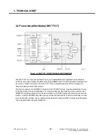
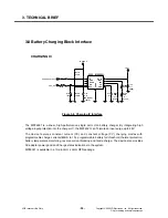
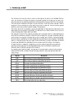
One PA block supports the GSM850 band and the other PA block supports the PCS1900 band. Both
PA blocks share common power supply pads to distribute current.
The output of each PA block and the outputs to the two receive pads are connected to the antenna
pad through PHEMT RF switches and a diplexer. The GaAs ddie, PHEMT die, Silicon (Si)die and
passive components are mounted on a multi-layer laminate substrate. The assembly is encapsulated
with plastic overmold.
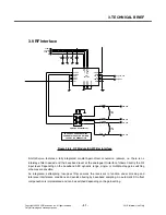
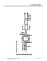
Band Selection and control of transmit and receive modes are performed using two external control
pads. Refer to the functional block diagram in Figure 3-2. The Band select pad (BS) selects between
GSM and PCS modes of peration. The transmit enable (TX_EN) pad controls receive or transmit mode
of the respective RF switch (TX = logic 1). Proper timing between transmit enable (TX_EN) and Analog
Power Control (VRAMP) allows for high isolation between the antenna and TX-VCO while the VCO is
being tuned prior to the transmit burst.
The SKY77517 is compatible with logic levels from 1.2V to VCC tor BS and TX_EN pads, depending
on the level applied to the VLOGIC pad. This feature provides additional flexibility for the designer in
the selection of FEM interface control logic.


