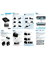
background image

C D - RW/DVD-ROM DRIVE

S E RVICE MANUAL

MODEL: GCC-4520B

MODEL : GCC-4520B

website http://biz.LGEservice.com

e-mail http://www.LGEservice.com/techsup.html

P/NO : 3828HS1041G

J u l y, 2003

Printed in Korea

Summary of Contents for GCC-4520B

Page 1: ...CD RW DVD ROMDRIVE SERVICE MANUAL MODEL GCC 4520B MODEL GCC 4520B website http biz LGEservice com e mail http www LGEservice com techsup html P NO 3828HS1041G July 2003 Printed in Korea ...

Page 2: ...nction of PCA and PMA area 20 9 OPC and ROPC 20 10 Writing Process of DISC 21 11 Super link 22 12 Zone CLV Recording 22 13 Optimum record speed 22 DVD CD DATA PROCESSING 23 26 1 Data Processing Flow 23 2 Copy Protection and Regional Code Management Block 24 3 About Prevention the DVD ROm from to be copy 25 4 About the DVD ROM Regional Code 26 INTERNAL STRUCTURE OF THE PICK UP 27 29 1 Block Diagram...

Page 3: ...LV 24X PCAV 4 Sustained Transfer rate Max 7 800Kb s CD ROM Max 52X Max 21 600Kb s DVD ROM Max 16X 5 PIO Mode 4 6 Multimedia MPC 3 Spec compliant 7 Support CD TEXT read 5 Audio 1 Output 16 bit digital data over ATA interface 2 Software Volume Control 3 Equipped with audio line output and headphone jack for audio CD playback 4 Front panel Volume Control for Headphone Output This service manual provi...

Page 4: ...ket writing Multi session 4 Cache memory R W 2 Mbyte 5 Disc diameter 12cm 8cm 6 Data capacity Yellow Book User Data Block 2 048 bytes block Mode 1 Mode 2 Form 1 2 336 bytes block Mode 2 2 328 bytes block Mode 2 Form 2 2 352 bytes block CD DA DVD ROM Book A B 2 048 bytes block 7 Rotational Speed CD CD Audio Analog 4X 10X CAV Approx 2 000 rpm CD Audio Digital 18X 40X CAV Approx 9 000 rpm CD R RW dat...

Page 5: ...le Layer 120ms Typ 200ms Typ 3 Data Buffer Capacity 2 Mbytes 5 POWER REQUIREMENTS 1 Voltage 5 V DC with 5 tolerance less than 100 mVp p Ripple voltage 12 V DC with 5 tolerance less than 100 mVp p Ripple voltage 2 Current Hold Track State 5V DC 1 3A 12 V DC 1 3A Max Seeking Spin up 5V DC 1 3A 12 V DC 1 3A Max 6 AUDIO PERFORMANCE Item Typical Limit Test Signal Test Condition Note OutputLevel 0 7 Vrm...

Page 6: ...essing it again will open the tray 3 Emergency Eject Hole Insert a paper clip here to eject the Disc tray manually or when there is no power 4 Volume control This is used to adjust the output volume of the headphone jack It can t be used to adjust the output volume for the audio output connectors on the rear panel NOTE Turn the volume down before turning on the power Sudden loud noises can damage ...

Page 7: ... damage the system Always turn the power OFF when connecting or disconnecting the cable 3 Jumper Connector This jumper determines whether the drive is configured as a master or slave Changing the master slave configuration takes effect after power on reset 4 Analog Audio Output Connector Provides output to a sound card analog signal Generally you need this to play a regular audio CD 5 Digital Audi...

Page 8: ...uit Board A Remove the Cabinet in the direction of arrow 4 See Fig 1 3 B Release 2 hooks a and remove the CD Tray drawing forward C Remove the Main Circuit Board in the direction of arrow 5 D At this time be careful not to damage the 4 connectors are positioned at left and bottom sides of the Main Circuit Board 2 MECHANISM ASSY DISASSEMBLY 2 1 Pick up Unit A Release screws B B Separate the Pick up...

Page 9: ...2 2 Pick up A Release 1 screw C and remove the Pick up Pick up Unit Pick up C Fig 2 2 9 ...

Page 10: ...02 A01 021 028 401 032 401 020 021 050 400 022 413 413 413 001 413 430 010 009 420 008 011 012 005 035 016 015 004 006 A B C D E F G H 1 2 3 4 5 003 002 013 452 029 031 027 026 033 025 430 419 020 449 023 014 11 12 EXPLODED VIEW ...

Page 11: ...hanged conditions of disc and change in operating temperature Jitter The 16 value of the time variation between leading and trailing edges of a specific I3 I11 pit or land as measured by Time Interval Analysis Deviation The difference between a fixed value of Pit length and Land length TOC Table Of Contents in the Lead in Area the subcode Q channel contains information about the Tracks on the disc...

Page 12: ...pitch p Radial Direction Iw A O a a Groove Land Radial Error Signal The Groove wobble Average center Actual center CD ROM READ ONLY DISC a 30nm ITEM CD ROM CD R CD RW Standard Yellow Book Orange Book II Orange Book III Record Not available Write once Re Writeable Tracking Signal I11 Itop 0 6 0 6 0 55 M11 0 70 HF Modulation Read Laser Power mW 0 5 mW 0 7 mW 1 0 mW Jitter 35 nsec 35 nsec 35 nsec Ref...

Page 13: ...disc It is so called WORM Write Once Read Many CD It is composed of polycarbonate layer Organic dye layer Reflective layer and Protective layer Gold Silver Reflective layer is used to enhance the reflectivity According to the kinds of Organic dye layer it is divided by Green CD Gold CD Blue CD Laser Wavelength 780 nm Laser Power read 0 7 mW Recording Power 8x 14 20mW 16x 25 35mW 32x 40 50mW 40x 45...

Page 14: ... reading is enabled by the difference of reflectivity It is possible to overwrite about 1000 times Laser Wavelength 780 nm Laser Power Read 1 0mW Recording Power Erase 4 18mW Write 6 45mW When disc rewriting new data is overwritten previously recorded data Polycarbonate layer has a Pre Groove which make a track Lens H D Beam Spot Focusing Lens Laser Spot at Constant Read Intensity Reflected Light ...

Page 15: ...Spot Recorded Mark Reflected Light Signal Reflected Light Signal Below ORP Mark Too Short At Optimum Record Power ORP Above ORP Mark Too Long Time 6 Writing process of CD RW Disc Write Power Erase Power Read Power Groove Crystal Amorphous Amorphous Recorded state lower reflectivity Melting quenching Heating gradual cooling Crystal phase Erased state higher reflectivity ...

Page 16: ...Area Lead out Area Center hole Clamping and Label Area Information Area PCA PMA Test Area Count Area Diameter 15 mm Diameter 45 mm Diameter 120 mm Unrecorded Disc Tsl 00 35 65 Tsl 00 15 05 Tsl 00 13 25 Tsl 99 59 74 00 00 00 in out Test Area for performing OPC procedures Count Area to find the usable area immediately in T A Tsl start time of the Lead in Area as encoded in ATIP PMA Program Memory Ar...

Page 17: ...ad_In area so that general Driver can read it Because PCA and PMA area exist before Lead In area General CD Player or CD ROM Drive can t read these areas 9 OPC and ROPC 1 OPC Optimum Power Control This is the first step of writing process because CD writer has its own laser power value and media have different writing characteristics This is determined by the Writing characteristic speed temperatu...

Page 18: ...a close Reference B level value c Normalization of B level is used to eliminate the effect of reflectivity fluctuation The reflected B level value is normalized by the disc reflectivity itself CD R RW Media Write Strategy Determination PCA Test Area Program Area PMA Area Lead In Area Lead out Area OPC PCA Count Area ROPC Recording Capacity of CD R RW 74Minute Recording media 2048 Byte Sector X 75 ...

Page 19: ... R can be recorded by 52x there is a possibility to occur recording fail during record especially in high speed write Before recording Drive decides write speed by test During the high speed write Drive checks the record status and control the optimum record speed not to occur record fail We call it as Optimum record speed 2 During the record Drive check the ATIP and Servo error Drive thinks the c...

Page 20: ...ice EFM demodulator CiRC error correction Audio DAC C3 decoder Buffer Memory controller CSS controller Atapi interface control Data PLL Servo ADC Focus tracking control output Sled control output CAV Spindle control P up Unit IC200 RF AMP MT1616E CD DVD IC100 MT1618E TE CSO GEN FE GEN IC500 DRAM Flash ROM IC100 MT1628E ...

Page 21: ...he regional code and plays title in the case of allowed regional code only 2 Management of DVD Disc for the scrambled of data 1 DVD ROM and DVD player of host generate the KEY 1 respectively transfer to opposite part the KEY 2 is received recognizes the data transfer or not with this value and generates the bus key encoded the data 2 Encoded Disc Key and Title Key host is transfer with the bus Key...

Page 22: ...MPEG 2 board generates the challenge key 10 Byte and transfers to drive The board and drive generate key 1 5Byte with the challenge key respectively Of course the Algorithm generating the key 1 is not known 3 Compare with the generated key 1 if it corresponds each other the first step of authentication is completed This is a course to identify the MPEG 2 board with a drive 4 The second step of aut...

Page 23: ...UM PLW PNG NZL AUS 4 The disc has the regional code of 8 bit Example The disc manufactured in the U S A has the number one Transfer to MPEG 2 board reading the regional code Receiving data from the MPEG 2 board and output through the monitor If the board is setting to the regional code 1 for the U S A Check the received regional code to number 1 all or not transfer the data to VGA card in accordan...

Page 24: ... J1 30 EDIS J1 29 RDIS J1 28 W2DIS J1 27 W1DIS J1 26 GND LD_HF J1 25 W2SET J1 24 W1SET J1 23 ESET J1 22 RSET J1 21 TEMP J1 20 Vcc HF J1 19 Vcc LD FM J1 18 VR J1 17 PD J1 16 LD J1 15 Vcc OEIC J1 14 GND OEIC J1 13 RF J1 12 RF J1 11 EF2 J1 10 B J1 9 A J1 8 EF1 J1 7 EF4 J1 6 C J1 5 D J1 4 EF3 J1 3 SW J1 2 Vc OEIC J1 1 A1 A7 220p 220p 220p 220p 2 7K 0 1u 1 2 3 4 5 6 7 16 15 14 13 12 11 10 9 8 D R14 22 ...

Page 25: ...lifier 22 ESET I input voltage for current amplifier 23 W1SET I input voltage for current amplifier 24 W2SET I input voltage for current amplifier 25 GND LD HF ground connection for LD IC and HF signal 26 W1DIS I Digital control of channel W1SET low active 27 W2DIS I Digital control of channel W2SET low active 28 RDIS I Digital control of channel RSET low active 29 EDIS I Digital control of channe...

Page 26: ...od A D B C k x EF1 EF4 EF2 EF3 This signal is generated in RF IC IC200 MT1616E and controls the pick up s left and right shift to find to track on Disc 3 RF Signal A B C D This signal is converted to DATA signal in DSP IC IC100 MT1628E 29 Pick Up module Photo Diode Tracking Focusing Infrared Iaser k F H E G A D B C A D B C k F H E G Offset TE Tp Sub2 Main Tp 2 Sub1 Track Center F E D C A B H G ...

Page 27: ...ite erase power control for CD R CD RW disc And the third APC loop is used for DVD read power control Owing to the small signal level in read power control mode the first APC loop amplifies x5 x10 x15 x20 the FMD signal FPDO to enhance the accuracy of read power control The register VRDCG 1 0 is used to adjust the gain of FMD signal The registers RDAC 7 0 and VBDAC 7 0 will set the read power leve...

Page 28: ...Focus Erro r Detector Track Error Detector A B C D E F G H IC200 MT1616E FE TE TE FE A D PARALLEL DIGITAL COMPENSATOR DAC SLED COMPENSATOR PWM FMSO FMSO2 IC100 Servo Control MT1618E Tracking x5 Focus x5 Tracking F ocusing Actuator FOSO TRSO F F T T Sled Control M Stepping Control Logic SL1 IC300 M63028FP SL1 SL2 SL2 IC300 M63028FP 27 12 28 13 18 14 1 2 MT1628E ...

Page 29: ...ual Layer DVD ROM Single Layer DVD ROM Movie Spindle Servo is controlled by IC100 MT1628E and servo signal is output via DMO pin 17 7 DVD 16x CAV Single Layer DVD ROM Data 32 A B D C E1 E2 E4 E3 F1 F2 F4 F3 Pick up IC200 MT1616E Wobble Signal Generator RF SRF EFM WOBSI Decode PLL Frequency Controller CD DSP SERVO LOCK DEFS MOTOR SPEE D CONTROLLER 174 FILTER TON DMSO ATIP CLV FG Level Shift Hall Se...

Page 30: ...36 35 34 33 32 31 30 29 28 27 26 25 24 23 22 21 20 19 18 17 16 15 14 13 12 11 10 9 8 7 6 5 4 3 2 1 65 66 67 68 69 70 71 72 73 74 75 76 77 78 79 80 81 82 83 84 85 86 87 88 89 90 91 92 93 94 95 96 97 98 99 100 101 102 GIO3 XRST WBLCLK WLDON IDGATE WFPDSH RLDON UDGATE RFPDSH H11T VF013 DVSS1 MCLK DVDD1 XLAT SCLK SDATA ASPREQ LRFZC BLANK DVDD2 SRVSH HTRC PHTO WBLSH DVSS2 GIO4 RFSUBO SUBGND2 OSCL2CP OS...

Page 31: ...ATIP Wobble 10 Bit ADC SBAD RFLVL AUX2 AUX1 WRFSUM FE DRCO2 CE TE SBAD RFLVL TEIN DEFECT RFZC1 TZC DFCTLP FOIP FOIN HAVC WBLSH SRVSH DRCO M FEO LRFZC BLANK SHPC SHBC PHTIN HTRC PHTO HTRLP VWDC1 VWDC1N FPDO FVREF VRDCN DVDLDO DVDMDI RFPDSH W FPDSH RLDON UDGATE WLDON IDGATE WRF AVDD1 AVSS1 AVDD2 AVSS2 AVDD3 AVSS3 AVDD4 AVSS4 AVDD5 AVSS5 AVDD6 AVSS6 AVDD7 AVSS7 DVDD1 DVSS1 DVDD2 DVSS2 DVDD SUBGND1 2 ...

Page 32: ...g Signal C 4 TRIND Analog Input Input of Tracking Signal D 127 FOIP Analog Input Input of Focusing Signal Positive 126 FOIN Analog Input Input of Focusing Signal Negative 47 SRVSH Digital Input TTL SMT S H Control Pulse of Main and Side Beam Signals 45 WBLSH Digital Input TTL SMT S H Control Pulse of Wobble Signal Focus Tracking Error Servo Control Signals 125 DRCO Analog Output Output of Differen...

Page 33: ...f RRF Signal 57 H11T VFO13 Digital Input TTL SMT 1 S H Control Pulse of WRF Signal 2 DVD RAM Header Signal ATIP Absolute Time In Pre groove 85 AGC1C Analog Output External Capacitor Connection of AGC1 in ATIP Block 84 AGC2C Analog Output External Capacitor Connection of AGC2 in ATIP Block 83 AGC3C Analog Output External Capacitor Connection of AGC3 in ATIP Block 65 ATFG Digital Output TTL 4 mA Dri...

Page 34: ... Signal Monitoring Serial Interface Other Digital Control Signals 50 ASPREQ Digital Output TTL 4 mA Driving ASP Request Signal Output to MT1618 for Sending Control Signals via Serial Interface 52 SCLK Digital Input TTL SMT Clock Input for Register Setting 51 SDATA Digital I O TTL 4 mA Driving Data Input Output for Register Setting 53 XLAT Digital Input TTL SMT Latch Input for Register Setting 63 X...

Page 35: ... Power Power Pin for Internal Analog Circuitry 5V 8 AVSS1 Analog Ground Ground Pin for Internal Analog Circuitry 107 AVDD2 Analog Power Power Pin for Internal Analog Circuitry 5V 103 AVSS2 Analog Ground Ground Pin for Internal Analog Circuitry 86 AVDD3 Analog Power Power Pin for Internal Analog Circuitry 5V 82 AVSS3 Analog Ground Ground Pin for Internal Analog Circuitry 29 AVDD4 Analog Power Power...

Page 36: ...32 131 130 129 128 127 126 125 124 123 122 121 120 119 118 117 116 115 114 113 112 111 110 109 RFIP RFIN RFDTSLVN SCOP SCON RFDTSLVP ADCVDD33 AMOP RFLEVEL FEI CSO TEI TEZISLV RFSUBI ADIN ADCVSS AMON PWM2VREF PWMVREF DVDD33 GIO3 WBLSH HRFZC SRVSH LRFZC BLANK ASPREQ XDATA DVDD33 XCLK XLAT DVDD25 XTALI XTALO DVSS H11T FO13 RFPDSH DVSS RLDON ICE WFPDSH WLDON 1DGATE WBLCLK XRST WBLSI PRST TEST HRST GIO...

Page 37: ...LPFIN LPFIP PLLVSS JITFN LPFON LPFOP LPION LPIOP JITFO DMO FG TEZISLV TEI HRFZC ADCVDD33 FEI TEI CSO RPLEVEL ADCVSS FOO TRO FMO FMO2 PWMOUT PWM2VREF PWMVREF XRST XLCK XLAT XDATA GIO LO DACVREF RO DACVDD33 DACVSS ADGO HD 15 0 PDIAG DASP HRST DIOW DIOR MACK HA 2 0 CS1FX CS3FX DMARQ IORDY INTRQ IOCS16 UPSEN UP3_2 UNIT0 UP3_3 UINT1 UALE UP0 7 0 UAD 7 0 UP2_7 UP2_0 UP3_5 UP3_4 UP3_1 UP3_0 UP3_6 UWR UP3...

Page 38: ...The positive output of data slicer current This pin is active when TRONS 1 Otherwise this pin is high inpedence 212 SCON Analog Output The negative output of data slicer current This pin is active when TRONS 1 Otherwise this pin is high inpedence 211 RFDTSLVP Analog Output The positive ouput of RF data slicer level 203 RFSUBI Analog Input RF subtraction signal input terminal 174 WBLSI 3 3V LVTTL W...

Page 39: ...og input General A D input 201 VDCVSS Ground Ground pin for ADC circuitry MOTOR 15 200 AMON Analog input Output Analog monitor negative pin 199 PWM2VREF Analog input A reference voltage input for PWM circuitry A typical value of 2 8v 198 PWMVREF Analog input A reference voltage input for PWM circuitry A typical value of 1 4v 209 AMOP Analog input Output Analog monitor positive pin 12 FOO Analog Ou...

Page 40: ...43 UA 7 4 3 3V LVTTL I O Lower address bus for external device Alternate function Internal monitored signal output Input mode is for MT1618 test only Defult 8mA 42 41 UA 3 0 3 3V LVTTL I O Lower address bus output for external device 39 38 Alternate function Internal monitored signal output Input mode is for MT1618 test only Default 8mA 30 UP3_7 URD 3 3V LVTTL I O Programmable bi directional I O A...

Page 41: ...ata bus output for external device Default 8mA Write Strategy 5 32 WXR Laser diode write power control output Write Read mode SW signal Default 8mA 33 ODON Laser diode over drive control output Over drive control SW signal Default 8mA 34 OSCEN High frequency modulation enable signal output Module control SW signal 35 CMOD High frequency modulation mode selection signal output 36 CFREQ Frequency se...

Page 42: ...t to CS pin of first SDRAM Default 4mA slew rate 88 RAS RAM Row Address Strobe This active low output is the Row Address Strobe signal to the RAM For SDRAM application this pin is row address strobe signal output connected to SDRAM Default 4mA slew rate 90 CASL Column Address Strobe Low Column Address Strobe When two column address strobe pins are used this pin is the Column Address Strobe Low sig...

Page 43: ...ce 6 122 ADGO Digital Audio Output The signal is the Digital Audio Output which supplies the IEC 958 digital audio data Default 2mA 127 DACVDD33 Analog Power 3 3V Power supply for internal audio DAC circuitry 126 RO Analog Output Right channel of audio 125 DACVREF Analog Output Reference voltage for external audio filter circuit 124 LO Analog Output Left channel of audio 123 AUDACVSS Ground Ground...

Page 44: ...Ultra DMA data strobe this signal is the data out strobe signal from the host for an Ultra DMA data out burst 143 IORDY I O Channel Ready Ultra DMA ready Ultra DMA data strobe For I O channel Ready this signal is negated to extend the host transfer cycle of any register read or write when the device is not able to complete the transfer For Ultra DMA Ready this is asserted by the device to indicate...

Page 45: ...nt signal PHTO from 1616 TEST 2 173 PRST Power on reset input high active 172 TEST Test mode active high RF SIO 5 191 ASPREQ ASP request signa input from MT1616 to get RECD1 XTOR DEFECT automatically 175 XRST RF reset output Active low 190 XDATA Data signal output for RF register setting 187 XLAT Latch signal output for RF register setting 188 XCLK Carrier clock signal output for RF register setti...

Page 46: ...wer 3 3V VDD for Input pad 37 83 136 186 DVDD25 Power 2 5V VDD for internal circuit 27 58 80 111 DVDD33 Power 3 3V VDD for output pad 142 165 189 31 61 89 105 DVSS Ground VSS for IO pad 139 154 180 40 86 133 183 DVSS Ground VSS for internal circuit ...

Page 47: ... 1 10 SL1 Slide inverted output 1 11 GND GND 12 W Motor drive output W 13 V Motor drive output V 14 U Motor drive output U 15 RSP Spindle current sensie 16 HW HW sensor amp input 17 HW HW sensor amp input 18 HV HV sensor amp input 19 HV HV sensor amp input 20 HU HU sensor amp input 21 HU HU sensor amp input Terminal Symbol Termianl function 42 OSC PWM carrier oscilation set 41 MU1 mute break selec...

Page 48: ...l input mode Power Is the pin 3 of IC902 3 3V Is the pin 3 of IC901 2 5V Reference 1 4V V14 check pin 1 of IC202 1 4V V14REF check pin 89 of IC200 2 0V V20REF check pin 88 of IC200 2 0V VHAVC check pin 91 of IC200 2 5V VFVREF check pin 92 of IC200 2 8V V28REF check pin 90 of IC200 NO NO YES YES YES YES 51 Are the X101 oscillating Check the X101 33 86MHz Check the IC100 NO Check the IC902 Check the...

Page 49: ...te continuously and the drive recognize the disc Does Disc rotate continuously and the drive recognize the disc After eject the tray Insert DVD disc and check rotation Does Disc rotate continuously and drive recognize the disc Go to Sled operating is abnormal Go to Recognition fail Case2 Blank CD R RW Go to Recognition fail Case 3 DVD Disc NO Go to Focus Actuator operating is abnormal NO Go to Las...

Page 50: ... Check the connection of IC200 pin 71 72 NO NO Check the Tray Connector CN104 Check the Motor Line and Motor YES Is there Tray control signal input IC300 pin 40 Check the connection of IC100 pin 19 Replace the IC100 Check the communication line between IC300 and IC100 NO YES YES YES When CN104 is open Is there Tray drive signal output Replace the IC300 NO YES 1 When there is no disc in drive MUTE1...

Page 51: ...00 pin 41 Check the connction of IC300 pin 1 2 Replace the IC300 Check the R305 R306 Check the connection of IC200 pin 71 72 Is there Sled drive voltage output CN102 pin 1 2 3 4 Replace the Sled Motor YES NO NO YES YES Check the Connection CN102 NO Is there Sled drive voltage input IC300 pin 1 2 YES NO Is there Sled drive voltage output IC300 pin 5 6 9 10 YES NO ...

Page 52: ...k the connection of IC100 pin 17 Replace the IC100 Is there Spindle drive voltage output IC300 pin 12 13 14 Check the Spindle Connector CN103 Replace the Spindle Motor NO NO YES YES Is there FG signal input IC100 pin 20 NO YES Check the connection of IC300 pin 24 Replace the IC300 OK ...

Page 53: ...r operating is abnormal Is there Focus Search control signal input IC300 pin 27 Is MUTE1 signal H IC300 pin 41 ReplacetheIC300 Check the connection CN101 pin35 36 CheckthePick upConnector CN101 Check the connection of IC200 pin 71 72 Replace the IC200 NO YES Replace the Pick Up Is there Focus Search drive voltage output IC300pin34 35 NO Check the connection of IC100 pin 12 Check the communication ...

Page 54: ...Pickup RF signal RFO was 500 900mVpp NO Go to LD CHECK YES NO ReplaceIC200 YES Check RFOP waveform IC200 Pin 30 was 1300 1700mVpp NO Goto TrackingServoisunstable YES YES Check after replacing IC100 It is OK NO Recognition Fail Case2 Blank CD R RW Is there WOBSI IC100 174 signal Check the connection between IC100 and IC200 Replace IC200 Replace the IC100 NO YES Is there ATFG IC200 pin65 signal NO Y...

Page 55: ...nition Fail Case 3 DVD Disc Replace the IC200 Replace the Q601 YES YES NO NO NO Is there RF signal at CN101 Pin11 YES Replace the Pickup NO Replace the IC200 Is there RF signal at IC200 Pin30 RFOP and Pin31 RFON YES NO Replace the IC100 Check again after the replace IC200 It is OK OK ...

Page 56: ...0 Check the connection between IC100 Pin205 and IC200 Pin 121 NO Is TE signal input normal in Focusing ON and Tracking OFF IC100 pin 205 NO Replace the IC100 Check the Drive IC IC300 and P U referring to Focus Actuator operating is abnormal Is there TRO signal output in Tracking ON IC100 pin13 NO Is PICK UP E F G H output normal CN101 pin 3 6 7 10 YES YES YES NO ...

Page 57: ...arameters of How to use Test Tool Execute D Laser Inspection of How to use Test Tool YES Laser operating is abnormal At Test CD Read Power NG E Normal F Execute C Laser Power Setup of How to use Test Tool NO YES NO NO At Test CD Write power NG YES ...

Page 58: ...IC200 Pin 26 Check and replace the IC200 RF YES IC200 Pin 114 FPDO 2 4 0 095V NO Check the connection of IC200 pin 114 Check and replace the CN101 Pick up YES Execute D Laser Inspection of How to Test Tool Check the P U connector and then replace the P U YES YES YES Measured Power 800 1300µW CN101 Pin 21 VRDC 220 50mV NO Check the connection of IC200 pin 104 Check and replace the IC200 ...

Page 59: ...00 Check the P U connector and then replace the P U Execute D Laser Inspection of How to use Test Tool YES YES YES NO Check the connection of IC200 pin 26 Check and replace the IC200 RF CN101 Pin 30 ENBL H YES NO Check the connection of IC200 pin 114 Check and replace the CN101 Pick up IC200 Pin 114 FPDO 2 0 0 3V YES NO NO NO Measured Power 28 32mW Normal Normal LD CHECK Not Recorded 62 ...

Page 60: ...the disc has long width Scratch change it Does the disc have any Dust Scratch Fingerprint YES NO Use LG bundle Software Write Tool Version Easy CD Creator Direct CD Nero InCD Is the write Tool version supported by LG CD RW DVD ROM Drive YES NO NO Check disc information on Writng Tool If you get some data information with Non Recordable Disc Message the disc is finalized Finalized Disc unrecordable...

Page 61: ...ritten file read normally Is the re written file read normally Is RFPDSH input signal Pulse when CD R writing IC200 pin 58 Does the blink of LED 801 occurs during Writing Do the IC200 RF pin 75 output toggle signals during Writing Check the connection between IC200 pin 75 and LED Check and replace the LED701 YES YES YES YES YES NO NO Check the communication lines between IC100 and IC200 Check and ...

Page 62: ...sc Adjust H P volume max HP801 NO AUD_MUTE L IC200 Pin 70 Do LOUT ROUT signals output IC100 Pin 124 126 Do audio Line signals output JK801 and CN100 pin 51 pin54 NO NO Check and replace the HP801 Does the audio signal output at the headphone jack HP801 NO Check and replace the IC800 Do audio signals output IC800 Pin1 7 NO YES YES YES YES YES Normal ...

Page 63: ... is displayed so you identify the proper device by model name GCC 4520B 4 Select ALPC B Check ALPC Parameters 1 Click button ALPC Parameters CD Read DAC h 001E to h 00C8 VWDC1 SL LO h 0050 to h 00C8 VWDC1 SL HI h 0050 to h 00C8 VWDC1 DAC200 h 0258 to h 0BB8 VWDC2 offset h FFFFFF88 to h 0050 VWDC2 h 0064 to h 0190 DVD Read DAC h 0032 to h 00C8 How to use Test Tool ...

Page 64: ...ult in the displyed message box Caution wavelength 780nm 4 A total power measurement is five times 5 After the measurement the result will be displayed 6 Click DVD button 7 Measure LD Power with LD Powermeter Type the result in the displyed message box Caution wavelength 650nm 8 A total power measurement is two times 9 After the measurement the result will be displayed 67 ...

Page 65: ...tween 800µW and 1300µW Test CD Write Power 5 Click CD Write LD ON button on menu 6 Enter 30 at displayed dialog box 7 Mesure LD Power with LD Powermeter Caution wavelength 780nm 8 Verify whether the laser power is between 28mW and 32mW Test DVD Read Power 9 Click DVD Read LD ON button on menu 10 Measure LD Power with LD Powermeter Caution wavelength 650nm 11 Verify whether the laser power is betwe...

Page 66: ...33 868MHz Servo S H Write S H Signal EQRF SBAD FEI TEI CSI ATFG I F cable Add Data H O S T VWDC VRDC FPD ABCD EFGH IC 200 IC 100 IC 500 IC 300 IC 201 M FG Tray Motor FOO TRO SLO PWM DMO Drive Mute IC 700 Add Data 2MB SDRAM LD Drive AT93C66 4KB EEPROM M63028FP 5Ch Servo DRIVE LED Control Mechanism S W Detect 39SF040 512KB Flash ROM Audio Mute Circuit Audio L R Line Out 3 3V 3 3V Reg 2 5V 5V GND GND...

Reviews: