background image

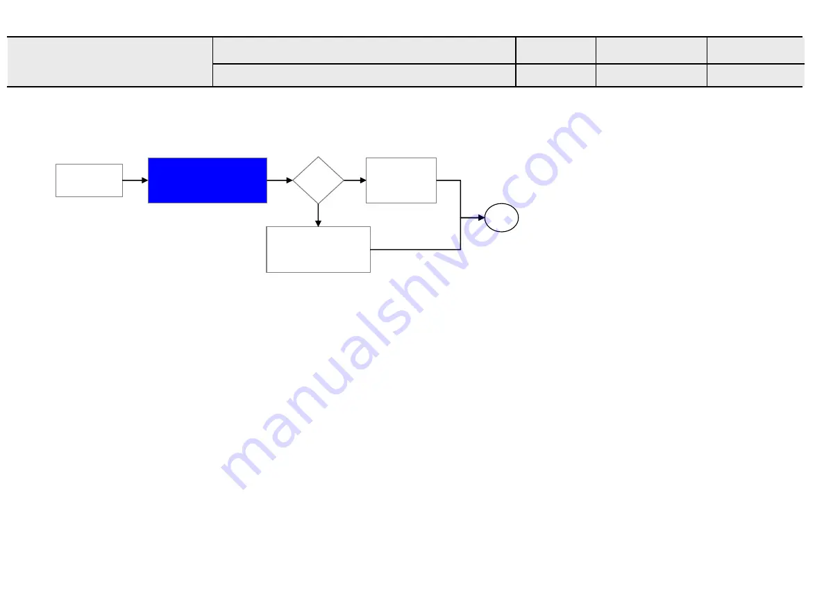
Check various 

voltages of Power 

Board ( 3.5V,12V, 24V) 

No Video/ 

No audio 

Check and 

replace 

MAIN B/D 

Replace Power 

Board and repair 

parts 

Standard Repair Process 

A. Video error 

 No video/ No audio  

A4 

Established 
date  

Revised date  

2/14 

End 

Normal 

Voltage 

Error symptom 

Copyright © 2015 LG Electronics. Inc. All rights reserved. 

Only for training and service purposes

LGE Internal Use Only

Summary of Contents for 43LF5700

Page 1: ...700 43LF5700 TA 43LF5710 43LF5710 TB CAUTION BEFORE SERVICING THE CHASSIS READ THE SAFETY PRECAUTIONS IN THIS MANUAL LED TV SERVICE MANUAL North Latin America http aic lgservice com Europe Africa http eic lgservice com Asia Oceania http biz lgservice com Internal Use Only ...

Page 2: ...ights reserved Only for training and service purposes CONTENTS CONTENTS 2 SAFETY PRECAUTIONS 3 SERVICING PRECAUTIONS 4 SPECIFICATION 6 ADJUSTMENT INSTRUCTION 9 BLOCK DIAGRAM 14 EXPLODED VIEW 17 SCHEMATIC CIRCUIT DIAGRAM APPENDIX TROUBLE SHOOTING GUIDE APPENDIX ...

Page 3: ...inals etc to be sure the set is safe to operate without damage of electrical shock Leakage Current Cold Check Antenna Cold Check With the instrument AC plug removed from AC source connect an electrical jumper across the two AC plug prongs Place the AC switch in the on position connect one lead of ohm meter to the AC plug prongs tied together and touch other ohm meter lead in turn to each exposed m...

Page 4: ...ctrostatic charge on your body by touching a known earth ground Alter natively obtain and wear a commercially available discharg ing wrist strap device which should be removed to prevent potential shock reasons prior to applying power to the unit under test 2 After removing an electrical assembly equipped with ES devices place the assembly on a conductive surface such as aluminum foil to prevent e...

Page 5: ...he solder joints of the two original leads If they are not shiny reheat them and if necessary apply additional solder Fuse and Conventional Resistor Removal Replacement 1 Clip each fuse or resistor lead at top of the circuit board hollow stake 2 Securely crimp the leads of replacement component around notch at stake top 3 Solder the connections CAUTION Maintain original spacing between the replace...

Page 6: ...g system 1 PAL B G D K I SECAM B G D K 2 NTSC M 3 DVB T 4 DVB T T2 5 DVB T T2 S2 1 Support all model 2 Support all model 3 depend on model 4 depend on model 5 depend on model 3 Channel Storage 1 DVB T Analog TV 1500EA 2 DVB T T2 Analog TV 1500EA 3 DVB T T2 S2 Analog TV 6000EA Satellite Digital TV VHF UHF C Band Ku Band Digital TV VHF UHF Analogue TV VHF UHF CATV 4 Receiving system Analog VHF UHF C...

Page 7: ...0 74 25 HDTV 720P 8 1280 720 45 00 60 00 74 25 HDTV 720P 9 1280 720 44 96 59 94 74 176 HDTV 720P 10 1920 1080 28 125 50 00 74 25 HDTV 1080I Except HD Model 11 1920 1080 33 75 60 00 74 25 HDTV 1080I Except HD Model 12 1920 1080 33 72 59 94 74 176 HDTV 1080I Except HD Model 13 1920 1080 56 25 50 00 148 50 HDTV 1080P Except HD Model 14 1920 1080 67 50 60 00 148 50 HDTV 1080P Except HD Model 15 1920 1...

Page 8: ...480 31 5 60 00 27 027 3 720 480 31 469 59 94 27 00 4 720 480 31 50 60 00 27 027 5 720 576 31 250 50 00 27 00 6 1280 720 37 50 50 00 74 25 7 1280 720 45 00 60 00 74 25 8 1280 720 44 96 59 94 74 176 9 1920 1080 28 125 50 00 74 25 10 1920 1080 33 75 60 00 74 25 11 1920 1080 33 72 59 94 74 176 12 1920 1080 56 250 50 00 148 50 13 1920 1080 67 50 60 00 148 50 14 1920 1080 67 432 59 94 148 35 15 1920 108...

Page 9: ... check OK message If Error is displayed check connection between computer jig and set 3 Click Read tab and then load download file XXXX bin by clicking Read 4 Click Connect tab If Can t is displayed check connection between computer jig and set 5 Click Auto tab and set as below 6 Click Run 7 After downloading check OK message USB DOWNLOAD epk file download 1 Put the USB Stick to the USB socket 2 A...

Page 10: ...de by pushing ADJ key Enter Internal ADC mode by pushing key at 8 ADC Calibration Caution Using P ONLY key of the Adjustment remote control power on TV ADC Calibration Protocol RS232 Adjust Sequence aa 00 00 Enter Adjust Mode xb 00 40 Component1 Input 480i ad 00 10 Adjust 480i Comp1 aa 00 90 End Adjust mode Required equipment Adjustment remote control 4 2 Function Check 4 2 1 Check display and sou...

Page 11: ...in B Gain should be kept on 0xC0 and adjust other two lower than C0 When R G B Gain are all C0 it is the FULL Dynamic Range of Module Full White Pattern CA 210 COLOR ANALYZER TYPE CA 210 RS 232C Communication Mode Color Temp Color coordinate Remark Cool C50 13 000 K X 0 271 0 002 Y 0 270 0 002 Test Signal Inner pattern for W B adjust External white pattern 80IRE 204gray Medium 0 9 300 K X 0 286 0 ...

Page 12: ...m the target value x y 1 x y target i Decrease the R G 2 x y target i First decrease the B gain ii Decrease the one of the others 3 x target y target i First decrease B so make y a little more than the target ii Adjust x value by decreasing the R 4 x target y target i First decrease B so make x a little more than the target ii Adjust x value by decreasing the G After You finish all adjustments Pre...

Page 13: ...1 5 KV min at 100 mA SIGNAL 3 KV min at 100 mA 2 2 Poles SIGNAL 3 KV min at 100 mA 2 TEST time 1 second 3 TEST POINT 1 3 Poles GND Test POWER CORD GND and SIGNAL CABLE GND Hi pot Test POWER CORD GND and LIVE NEUTRAL 2 2 Poles Hi pot Test Accessible Metal and LIVE NEUTRAL 4 LEAKAGE CURRENT At 0 5 mArms NO Item CMD 1 CMD 2 Data 0 Enter download Mode Download Mode In A A 0 0 When transfer the Mode In...

Page 14: ... SDA NAND FLASH 1Gbit IC102 PCM_A 0 7 RXA0 RXA4 RXACK RXB0 RXB4 RXBCK SPK_R SPK_L AMP_SCL SDA AUD_MASTER_CLK AUD_LRCH AUD_LRCK AUD_SCK STA380BW IC3401 Connector P600 KEY1 2 LED_R IR REAR HDMI1 JK801 Main SOC M1A 256MB T IC101 SPDIF_OUT SPDIF Optic JK1001 COMP2_L R_IN COMP2_Y AV_CVBS_IN COMP2_Pb Pr AV2_L R_IN AV2_CVBS_IN Comp1 AV1 JK1701 AV2 TU_SCL SDA SIF D_IF CVBS SIDE USB JK700 HDMI2 MHL JK803 C...

Page 15: ...s reserved Only for training and service purposes 2 I2C HW_I2C SW_I2C SW_I2C TUNER AMP DEMOD LNB EEPROM Digital_Eye HW I2C 4ea SW I2C 1ea HW_I2C I2C_SC D KM3 I2C_DDCR_CK GPIO76 77 SCK D M0 GPIO58 59 I2C_SC D KM1 GPIO80 81 GPIO159 160 SDAM2 GPIO55 56 HW_I2C URSA VCOM ...

Page 16: ... Only for training and service purposes 3 POWER 13 2V AVDD_NODIE AVDD_DMPLL AVDD_AU33 Tuner 3 3V 1 10V_VDDC L412 IC405 DCDC 13 2V 3 5V L410 3 3V_Normal L404 13 2V_AMP PANNEL Vcc L5600 L408 L206 L207 L205 L205 IC400 DCDC 13 2V 3 5V 5V_Normal 3 3V_Normal IC404 LDO 3 3V 1 5V DDR ...

Page 17: ...ectrical and mechanical parts in this chassis have special safety related characteristics These parts are identified by in the Schematic Diagram and EXPLODED VIEW It is essential that these special safety parts should be replaced with the same components as recommended in this manual to prevent Shock Fire or other Hazards Do not modify the original design without permission of manufacturer IMPORTA...

Page 18: ...S_DATA 5 PCM_D 2 PCM_A 14 CI_TS_DATA 4 SCART1_Lout PCM_REG HP_ROUT PCM_IOWR CI_TS_DATA 1 PCM_RST PCM_A 12 CI_TS_VAL CI_TS_DATA 3 PCM_WAIT SCART1_Rout CI_TS_DATA 6 PCM_D 4 PCM_A 8 DTV MNT_VOUT PCM_D 7 PCM_OE SIDE_HP_MUTE CI_TS_DATA 7 PCM_IORD PCM_A 11 SC1_B COMP1_Pb SC1_G COMP1_Y SC1_R COMP1_Pr SC1 COMP1_L_IN SC1 COMP1_DET SC1 COMP1_R_IN FE_TS_DATA 1 FE_TS_DATA 2 FE_TS_DATA 3 FE_TS_DATA 4 FE_TS_DAT...

Page 19: ...ormal ZD401 2 5V 1 10V_VDDC C408 2200pF 50V OPT C417 3300pF 50V C405 10uF 25V C421 0 047uF 25V L404 CB2012PK501T C409 2200pF 50V OPT C416 22pF 50V C411 82pF 50V OPT C424 22uF 16V 13 2V R403 10K C419 22pF 50V C412 10uF 6 3V OPT C406 10uF 25V 3 3V_Normal C410 0 047uF 25V 3 3V_Normal C420 3300pF 50V R408 100K C407 1uF 10V R407 4 7K OPT R409 91K 5V_Normal L413 2uH L405 4 7uH L406 4 7uH ZD402 1 TVS_KEC...

Page 20: ... _HDMI4 R815 100 HDMI 2 C800 0 047uF 25V HDMI 2_MHL D2 _HDMI4 R802 1 8K D2 _HDMI2 R808 10K HDMI_CEC D0 _HDMI4 VA806 ESD_HDMI2 JK801 EAG62611204 HDMI 2 14 NC 13 CE_REMOTE 5 D1_GND 20 GND 12 CK 11 CK_GND 2 D2_GND 19 HP_DET 18 5V 10 CK 4 D1 1 D2 17 GND 9 D0 8 D0_GND 3 D2 16 DDC_DATA 7 D0 6 D1 15 DDC_CLK JK801 1 DAADR019A HDMI 2_EMI_FOOSUNG 14 RESERVED 13 CEC 5 TMDS_DATA1_SHIELD 20 BODY_SHIELD 12 TMDS...

Page 21: ...ONLY MANUFACTURES SPECIFIED PARTS BE USED FOR THE CRITICAL COMPONENTS IN THE SYMBOL MARK OF THE SCHEMETIC SPDIF 2014 06 02 10 L14_CA_M1A 3 3V_Normal SPDIF_OUT JK1001 JST1223 001 SPDIF_OPTIC 1 GND 2 VCC 3 VINPUT 4 FIX_POLE C1001 1uF 10V OPT C1002 18pF 50V SPDIF_OPTIC SPDIF ESD Ready Copyright 2015 LG Electronics Inc All rights reserved Only for training and service purposes LGE Internal Use Only ...

Page 22: ..._DDR3_DQU 7 F20 ZQ E9 NT5CB64M16FP DH IC1201 1 DDR_1600_1G_NAN EAN61859502 A0 N3 A1 P7 A2 P3 A3 N2 A4 P8 A5 P2 A6 R8 A7 R2 A8 T8 A9 R3 A10 AP L7 A11 R7 A12 N7 NC_6 T3 NC_5 M7 BA0 M2 BA1 N8 BA2 M3 CK J7 CK K7 CKE K9 CS L2 ODT K1 RAS J3 CAS K3 WE L3 RESET T2 DQSL F3 DQSL G3 DQSU C7 DQSU B7 DML E7 DMU D3 DQL0 E3 DQL1 F7 DQL2 F2 DQL3 F8 DQL4 H3 DQL5 H8 DQL6 G2 DQL7 H7 DQU0 D7 DQU1 C3 DQU2 C8 DQU3 C2 D...

Page 23: ...FLASH 140721 13 L14_CA_M1A SPI_SCK 3 5V_ST 3 5V_ST C1300 0 1uF 16V R1301 4 7K OPT SPI_CS SPI_SDO R1302 33 R1300 10K OPT SPI_SDI FLASH_WP 3 5V_ST IC1300 MX25L8035EM2I 10G SPI_FLASH_MACRONIX 3 WP SIO2 2 SO SIO1 4 GND 1 CS 5 SI SIO0 6 SCLK 7 NC SIO3 8 VCC IC1300 1 W25Q80DVSSIG SPI_FLASH_WINBOND 3 WP IO2 2 DO IO1 4 GND 1 CS 5 DI IO0 6 CLK 7 HOLD IO3 8 VCC Serial Flash for SPI boot Copyright 2015 LG El...

Page 24: ... 0 IF_NON_FILTER_KR C1614 20pF 50V OPT TU_SCL TU_GND_A R1608 33 RF_SWITCH_CTL C1607 0 1uF 16V FE_TS_SYNC R1611 1 1K TU_IIC_NON_ATSC_1K 3 3V_Normal FE_TS_CLK R1610 1 8K TU_IIC_ATSC_1 8K R1612 0 OPT R1613 0 OPT TU_CVBS TU_SIF TU_GND_A C1617 1000pF 630V TU_GND_Cap TDJH H301F TU1601 TU_ATSC 47 SHIELD 6 DIF P 7 DIF N 8 SIF 9 CVBS 1 3 3V 2 NC_1 3 DIF_AGC 4 SCL_RF 5 SDA_RF A1 A1 B1 B1 TDJH G301D TU1601 1...

Page 25: ..._CVBS_ZENER_ROHM ZD1706 AV2_CVBS_ZENER_ROHM ZD1703 COMP_Pb_ZENER_ROHM ZD1702 COMP_Pb_ZENER_ROHM ZD1701 COMP_Pr_ZENER_ROHM ZD1707 1 AV2_CVBS_ZENER_KEC ZD1706 1 AV2_CVBS_ZENER_KEC ZD1703 1 COMP_Pb_ZENER_KEC ZD1702 1 COMP_Pb_ZENER_KEC ZD1701 1 COMP_Pr_ZENER_KEC ZD1700 1 COMP_Pr_ZENER_KEC ZD1705 1 COMP_Y_ZENER_KEC ZD1704 1 COMP_Y_ZENER_KEC DTV MNT_VOUT R1723 75 CVBS_OUT_TEST R1724 0 CVBS_OUT_TEST JK17...

Page 26: ...P_LOUT R3004 1K HEAD_PHONE HP_DET 3 5V_ST HP_ROUT SIDE_HP_MUTE R3002 1K HEAD_PHONE C3002 1000pF 50V OPT R3003 1K HEAD_PHONE Q3002 MMBT3904 NXP OPT E B C Q3003 MMBT3904 NXP OPT E B C Q3005 MMBT3904 NXP OPT E B C Q3004 MMBT3904 NXP OPT E B C Q3001 MMBT3906 NXP OPT E B C Q3000 MMBT3904 NXP OPT E B C R3000 1K OPT C3004 4 7uF 10V HEAD_PHONE L3001 HEAD_PHONE 5 6uH L3000 HEAD_PHONE 5 6uH C3005 4 7uF 10V ...

Page 27: ...BE USED FOR THE CRITICAL COMPONENTS IN THE SYMBOL MARK OF THE SCHEMETIC RS232C_MSTAR_DEBUG_4P 2014 05 22 40 L14_CA_M1A PM_RXD 3 5V_ST R4001 100 R4000 100 P4000 12507WS 04L RS232C_DEBUG_4P 1 VCC 2 PM_RXD 3 GND 4 RM_TXD 5 GND PM_TXD JP_GND1 JP_GND3 JP_GND2 JP_GND4 RS 232C 4PIN RS 232C 4PIN MSTAR DEBUG 4PIN Copyright 2015 LG Electronics Inc All rights reserved Only for training and service purposes L...

Page 28: ...0 IR_Eye_Sensor R4600 3 3K R4607 1K IR_Eye_Sensor C4603 0 1uF 16V KEY1 3 5V_ST R4601 100 C4601 1000pF 50V KEY2 VA4600 OPT 5 6V R4604 10K 1 C4604 100pF 50V R4605 1K IR_Eye_Sensor SENSOR_SDA 3 3V_Normal P4601 12507WR 08L IR_8p 1 2 3 4 5 6 7 8 9 C4602 0 1uF 16V L4600 BLM18PG121SN1D C4605 18pF 50V IR_Eye_Sensor 3 5V_ST IR R4609 100 IR_Eye_Sensor 3 5V_ST R4606 1 8K SENSOR_SCL P4600 12507WR 10L IR_10p 1...

Page 29: ...GPIO176 R19 LVA2M TTL_B 7 POL GPIO177 P20 LVA1P TTL_G 0 EPI0 GPIO178 P19 LVA1M TTL_G 1 EPI0 GPIO179 N20 LVA0P TTL_G 2 EPI1 GPIO180 N21 LVA0M TTL_G 3 EPI1 GPIO181 N19 LVB4P TTL_G 4 EPI2 GPIO182 M21 LVB4M TTL_G 5 EPI2 GPIO183 M20 LVB3P TTL_G 6 EPI3 GPIO184 M19 LVB3M TTL_G 7 EPI3 GPIO185 L20 LVBCKP TTL_R 0 EPI4 GPIO186 L19 LVBCKM TTL_R 1 EPI4 GPIO187 K20 LVB2P TTL_R 2 EPI5 GPIO188 K21 LVB2M TTL_R 3 E...

Page 30: ...39 H12 GND_40 H13 GND_41 H14 GND_42 H15 GND_43 H16 GND_44 H17 GND_45 H18 GND_46 J7 GND_47 J8 GND_48 J9 GND_49 J10 GND_50 J11 GND_51 J12 GND_52 J13 GND_53 J14 GND_54 K8 GND_55 K10 GND_56 K11 GND_57 L10 GND_58 M5 GND_59 M7 GND_60 M8 GND_61 M9 GND_62 M10 GND_63 N4 GND_64 N5 GND_65 N6 GND_66 N7 GND_67 N8 GND_68 N9 GND_69 N10 GND_70 P4 GND_71 P5 GND_72 P6 GND_73 P7 GND_74 P9 GND_75 P10 GND_76 P15 GND_7...

Page 31: ...S 10 PLL_FLTM 11 PLL_FLTP 12 VR_ANA 13 AVDD 14 A_SEL_FAULT 15 MCLK 16 OSC_RES 17 DVSSO 18 VR_DIG 19 PDN 20 LRCLK 21 SCLK 22 SDIN 23 SDA 24 SCL 25 RESET 26 STEST 27 DVDD 28 DVSS 29 GND 30 AGND 31 VREG 32 GVDD_OUT 33 BST_D 34 PVDD_CD_1 35 PVDD_CD_2 36 OUT_D 37 PGND_CD_1 38 PGND_CD_2 39 OUT_C 40 NC_3 41 NC_4 42 BST_C 43 BST_B 44 NC_5 45 NC_6 46 OUT_B 47 PGND_AB_1 48 PGND_AB_2 49 EP C5614 0 1uF 16V 3 ...

Page 32: ...C7SZ08FU_TOSHIBA MHL_AND_GATE_TOSHIBA 3 GND 2 IN_A 4 OUT_Y 1 IN_B 5 VCC IC5801 1 74LVC1G08GW MHL_AND_GATE_NXP 3 2 4 1 5 AVDD5V_MHL 5V_HDMI_4 R5803 0 MHL_OCP R5802 10 5V_Normal IC5802 BD82020FVJ MHL_OCP 3 IN_2 2 IN_1 4 EN 1 GND 5 OC 6 OUT_1 7 OUT_2 8 OUT_3 R5804 10K MHL_OCP MHL_OCP_DET 3 3V_Normal C5802 0 1uF MHL_OCP R5805 100K OPT C5801 10uF 10V MHL_OCP MHL_5V_EN D5801 40V SS2040LL LG MHL_SUZHOU D...

Page 33: ...MPONENTS IN THE SYMBOL MARK OF THE SCHEMETIC 140707 USB_3216_CAP4 75 L14_CA_M1A JK700 3AU04S 305 ZC LG 1 2 3 4 5 D700 RCLAMP0502BA OPT SIDE_USB1_DM SIDE_USB1_DP ZD700 5V OPT SD05 C701 5pF 50V OPT C702 5pF 50V OPT 5V_USB C700 22uF 16V USB_CAP4 C703 22uF 16V USB_CAP2 C704 22uF 16V USB_CAP3 C705 22uF 16V USB_CAP1 R700 2 2 R701 2 2 USB 3216 CAP SIDE Copyright 2015 LG Electronics Inc All rights reserve...

Page 34: ...25 26 27 28 29 30 31 32 33 34 35 36 37 38 39 40 41 42 43 44 45 46 47 48 49 50 51 52 RXB1 RXB0 RXA4 RXA1 Pol change RXB4 RXACK RXBCK RXA0 RXA2 RXA2 RXBCK RXB4 RXA3 RXA1 RXB2 RXB3 RXA3 RXBCK RXACK RXA2 RXA1 RXB1 RXB3 RXA3 RXA2 RXA0 RXA4 Shift RXBCK RXB2 RXA4 51Pin LVDS Connector For FHD 60Hz RXACK RXA3 RXACK RXB3 RXA3 RXA1 RXB0 RXA0 RXACK RXB3 LVDS_SEL RXA4 RXB3 RXA4 RXA2 RXA2 RXA1 RXB2 Pol change R...

Page 35: ......

Page 36: ...L15 HD FHD Repair Process Copyright 2015 LG Electronics Inc All rights reserved Only for training and service purposes LGE Internal Use Only ...

Page 37: ... viewing power auto on off 8 8 C Audio error No audio Normal video 9 9 Wrecked audio discontinuation noise 10 10 D Function error Remote control Local switch checking 11 11 External device recognition error 12 12 E Noise Circuit noise mechanical noise 13 13 F Exterior error Exterior defect 14 First of all Check whether there is SVC Bulletin in GCSC System for these model Contents of Standard Repai...

Page 38: ...efore replacing the Main Board Replace Main Board Re enter White Balance value Precaution Established date Standard Repair Process Revised date 1 14 Error symptom A Video error No video Normal audio A4 A1 A2 A6 A3 First of all Check whether all of cables between board is inserted properly or not Main B D Power B D LVDS Cable Speaker Cable IR B D Cable Normal Audio On Y N Normal Voltage Normal Volt...

Page 39: ...AIN B D Replace Power Board and repair parts Standard Repair Process A Video error No video No audio A4 Established date Revised date 2 14 End Normal Voltage Y N Error symptom Copyright 2015 LG Electronics Inc All rights reserved Only for training and service purposes LGE Internal Use Only ...

Page 40: ...ing Y N Y Y By using Digital signal level meter By using Diagnostics menu on OSD Menu Set up Support Signal Test Signal strength Normal over 50 Signal Quality Normal over 50 Y Contact with signal distributor or broadcaster Cable or Air N N Y N A6 Standard Repair Process Established date Revised date 3 14 End Normal Signal Normal Picture Normal Picture Normal Picture SVC Bulletin End End Normal Pic...

Page 41: ...tting match with installed ANT N Y N A6 Standard Repair Process Established date Revised date 4 14 Check satellite setting Check LNB frequency Check satellite Check Satellite connection DiSEqC motor etc Contact with signal distributor or broadcaster Cable or Air N Check Tuner soldering Replace Main B D Normal Picture End Normal Picture Normal Setting SVC Bulletin Normal Signal End End Error sympto...

Page 42: ...in B D Replace Main B D N N A Video error Color error A7 N Y Replace module Request repair for external device cable Check Test pattern A10 A8 A9 Standard Repair Process Established date Revised date 5 14 End Color error Color error External device Cable Normal External device Cable Normal External Input Component error HDMI error Error symptom Copyright 2015 LG Electronics Inc All rights reserved...

Page 43: ... Main B D Check screen condition by input External Input Component RGB HDMI DVI Request repair for external device Connect other external device and cable Check normal operation of External Input Component HDMI by connecting Jig pattern Generator Set top Box etc Replace Main B D N Y Check S W Version Y N S W Upgrade Y N Y N Replace Main B D Replace Module Established date Revised date 6 14 Standar...

Page 44: ... each output of Power B D N Y Replace Main B D Y Replace Main B D N Y Check ST BY 3 5V Replace Power B D N Replace Power B D Y A11 A12 A13 A4 Standard Repair Process Established date Revised date 7 14 Stand By Red End Power LED On Normal Voltage Normal Voltage Normal Operation Error symptom Copyright 2015 LG Electronics Inc All rights reserved Only for training and service purposes LGE Internal Us...

Page 45: ...f by OFF TIMER POWEROFF_SLEEPTIMER Power off by SLEEP TIMER POWEROFF_INSTOP Power off by INSTOP KEY POWEROFF_AUTOOFF Power off by AUTO OFF POWEROFF_ONTIMER Power off by ON TIMER POWEROFF_RS232C Power off by RS232C POWEROFF_RESREC Power off by Reservated Record POWEROFF_RECEND Power off by End of Recording POWEROFF_SWDOWN Power off by S W Download POWEROFF_UNKNOWN Power off by unknown status except...

Page 46: ...ts Check Speaker disconnection N Y Replace Speaker Replace MAIN Board C Audio error No audio Normal video A15 A16 Established date Revised date 9 14 Standard Repair Process End Normal Voltage Off Disconn ection Error symptom Copyright 2015 LG Electronics Inc All rights reserved Only for training and service purposes LGE Internal Use Only ...

Page 47: ...ovider Y Check audio B Voltage 24V In case of External Input signal error Check and fix external device Replace Main B D N Established date Revised date 10 14 Standard Repair Process A16 End Signal Normal Normal Voltage Normal Audio Wrecked Audio Discontinuation Noise only for D TV Wrecked Audio Discontinuation Noise only for Analog Wrecked Audio Discontinuation Noise only for External Input N Rep...

Page 48: ...connection Connector solder Check B 3 5V On Main B D A17 N N Check 3 5v on Power B D Replace Power B D or Replace Main B D Power B D don t have problem A4 Check IR Output signal N Y Repair Replace IR B D N A17 Replace Main B D Y A17 Standard Repair Process Established date Revised date 11 14 End Normal Operating Normal Voltage Normal Signal Normal Operating Normal Operating End Y Error symptom Cop...

Page 49: ...h technical information D Function error External device recognition error Established date Revised date 12 14 Standard Repair Process Signal Input Technical information External Input and Component Recognition error HDMI Optical Recognition error Error symptom Copyright 2015 LG Electronics Inc All rights reserved Only for training and service purposes LGE Internal Use Only ...

Page 50: ...n manual For models without any fix information provide the description OR Mechanical noise is a natural phenomenon and apply the 1st level description When the customer does not agree apply the process by stage Describe the basis of the description in Part related to nose in the Owner s Manual E Noise Circuit noise mechanical noise Established date Revised date 13 14 Standard Repair Process Circu...

Page 51: ...stand F Exterior defect Exterior defect Established date Revised date 14 14 Standard Repair Process Module damage Cabinet damage Remote Controller damage Stand damage Error symptom Copyright 2015 LG Electronics Inc All rights reserved Only for training and service purposes LGE Internal Use Only ...

Page 52: ...eck Link Cable LVDS reconnection condition A8 A9 10 Adjustment Test pattern ADJ Key A10 11 A Video error_Vertical Horizontal bar residual image light spot Connection diagram A8 12 Check Link Cable LVDS reconnection condition A8 A9 13 Adjustment Test pattern ADJ Key A10 14 Appendix Defected Type caused by T Con Inverter Module Exchange T Con Board 1 A 1 5 15 Exchange T Con Board 2 A 2 5 16 Exchange...

Page 53: ... checking method A14 24 C Audio error_No audio Normal video Checking method in menu when there is no audio A15 25 Voltage and speaker checking method when there is no audio A16 26 C Audio error_Wrecked audio discontinuation Voltage and speaker checking method in case of audio error A16 27 D Function error_ No response in remote controller key error Remote controller operation checking method A17 C...

Page 54: ...ed eye A Video error_No video Normal audio ALL MODELS A1 Established date Revised date Error symptom Content Power On disjoint back case check lighting at 2 points Copyright 2015 LG Electronics Inc All rights reserved Only for training and service purposes LGE Internal Use Only ...

Page 55: ...t 13V from Power Board supply to inverter PCB Check Pin contacting statement and connection statement 1 Measure DC 24V applying to inverter PCB from Power Board 2 Output 24V from Power Board supply to inverter PCB Check Pin contacting statement and connection statement FHD HD UHD Error symptom Content Copyright 2015 LG Electronics Inc All rights reserved Only for training and service purposes LGE ...

Page 56: ...ual Check White Balance value A Video error_No video Normal audio ALL MODELS A3 Established date Revised date Entry method 1 Press the ADJ button on the remote controller for adjustment 2 Enter into White Balance of item 7 3 After recording the R G B GAIN Cut value of Color Temp Cool Medium Warm re enter the value after replacing the MAIN BOARD Error symptom Content Copyright 2015 LG Electronics I...

Page 57: ... 4 PDIM 1 5 3 5V 6 3 5V 7 GND 8 PDIM 2 9 24V 10 24V 11 GND 12 GND 13 12V 14 12V 15 12V 16 NC 17 GND 18 GND Check DC 3 5V 12V 24V 12 Pin Power Board Main Board SMAW200 H18S5 1 Power on 2 PDIM 2 3 GND 4 13 2V 5 13 2V 6 13 2V 7 13 2V 8 13 2V 9 GND 10 GND 11 DRV_ON 12 PDIM 1 UHD FHD HD Error symptom Content Copyright 2015 LG Electronics Inc All rights reserved Only for training and service purposes LG...

Page 58: ...15dB 20dB etc Standard Repair Process Detail Technical Manual TUNER input signal strength checking method A Video error_Video error video lag stop A5 Established date Revised date Error symptom Content Copyright 2015 LG Electronics Inc All rights reserved Only for training and service purposes LGE Internal Use Only ...

Page 59: ...o lag stop 1 Checking method for remote controller for adjustment Press the IN START with the remote controller for adjustment Version A6 Established date Revised date Error symptom Content Copyright 2015 LG Electronics Inc All rights reserved Only for training and service purposes LGE Internal Use Only ...

Page 60: ...dual image light spot As the part connecting to the external input check the screen condition by signal A7 Established date Revised date ALL MODELS The picture depends on model Error symptom Content Copyright 2015 LG Electronics Inc All rights reserved Only for training and service purposes LGE Internal Use Only ...

Page 61: ... Detail Technical Manual Check and replace Link Cable LVDS and contact condition A Video error_Color error ALL MODELS A8 A9 Established date Revised date Error symptom Content Copyright 2015 LG Electronics Inc All rights reserved Only for training and service purposes LGE Internal Use Only ...

Page 62: ... patterns using the ADJ Key Checking item 1 Defective pixel 2 Residual image 3 MODULE error ADD BAR SCAN BAR 4 Video error Classification of MODULE or Main B D A10 Established date Revised date Error symptom Content Copyright 2015 LG Electronics Inc All rights reserved Only for training and service purposes LGE Internal Use Only ...

Page 63: ...n Solder defect CNT Broken Solder defect CNT Broken Solder defect CNT Broken Abnormal Power Section Solder defect Short Crack Abnormal Power Section Solder defect Short Crack Appendix Exchange T Con Board 1 Copyright 2015 LG Electronics Inc All rights reserved Only for training and service purposes LGE Internal Use Only ...

Page 64: ...ower Section Solder defect Short Crack Fuse Open Abnormal power section Noise GRADATION GRADATION Abnormal Display Appendix Exchange T Con Board 2 Copyright 2015 LG Electronics Inc All rights reserved Only for training and service purposes LGE Internal Use Only ...

Page 65: ...pendix Exchange PSU LED driver No Light Dim Light Dim Light Dim Light No picture Sound Ok Copyright 2015 LG Electronics Inc All rights reserved Only for training and service purposes LGE Internal Use Only ...

Page 66: ...Press damage Crosstalk Crosstalk Press damage Panel Mura Light leakage Press damage Un repairable Cases In this case please exchange the module Copyright 2015 LG Electronics Inc All rights reserved Only for training and service purposes LGE Internal Use Only ...

Page 67: ...lock Source TAB IC Defect Horizontal Block Gate TAB IC Defect Horizontal line Gate TAB IC Defect Gate TAB IC Defect Horizontal Block Gate TAB IC Defect Appendix Exchange the Module 2 Un repairable Cases In this case please exchange the module Copyright 2015 LG Electronics Inc All rights reserved Only for training and service purposes LGE Internal Use Only ...

Page 68: ...LED B Power error _No power A11 Established date Revised date ST BY condition Red Front LED control Menu Option Standby Light On Off Error symptom Content Copyright 2015 LG Electronics Inc All rights reserved Only for training and service purposes LGE Internal Use Only ...

Page 69: ... date 18 Pin Power Board Main Board SMAW200 H18S5 1 Power on 2 DRV ON 3 3 5V 4 PDIM 1 5 3 5V 6 3 5V 7 GND 8 PDIM 2 9 24V 10 24V 11 GND 12 GND 13 12V 14 12V 15 12V 16 NC 17 GND 18 GND Check DC 3 5V 12V 24V Error symptom Content Copyright 2015 LG Electronics Inc All rights reserved Only for training and service purposes LGE Internal Use Only ...

Page 70: ...ower Board Main Board SMAW200 H18S5 1 Power on 2 DRV ON 3 3 5V 4 PDIM 1 5 3 5V 6 3 5V 7 GND 8 PDIM 2 9 24V 10 24V 11 GND 12 GND 13 12V 14 12V 15 12V 16 NC 17 GND 18 GND Check power on Pin 1 pin is high about 3 3V Error symptom Content Copyright 2015 LG Electronics Inc All rights reserved Only for training and service purposes LGE Internal Use Only ...

Page 71: ...t item 3 Standard Repair Process Detail Technical Manual POWER OFF MODE checking method B Power error _Off when on off whiling viewing ALL MODELS A14 Established date Revised date Error symptom Content Copyright 2015 LG Electronics Inc All rights reserved Only for training and service purposes LGE Internal Use Only ...

Page 72: ...ker Check Standard Repair Process Detail Technical Manual Checking method in menu when there is no audio C Audio error_No audio Normal video ALL MODELS A15 Established date Revised date Error symptom Content Copyright 2015 LG Electronics Inc All rights reserved Only for training and service purposes LGE Internal Use Only ...

Page 73: ...erminal the speaker is normal Standard Repair Process Detail Technical Manual Voltage and speaker checking method when there is no audio C Audio error_No audio Normal video ALL MODELS A16 Established date Revised date 18 Pin Power Board Main Board SMAW200 H18S5 1 Power on 2 DRV ON 3 3 5V 4 PDIM 1 5 3 5V 6 3 5V 7 GND 8 PDIM 2 9 24V 10 24V 11 GND 12 GND 13 12V 14 12V 15 12V 16 NC 17 GND 18 GND Error...

Page 74: ...rmal when the Analog Tester needle moves slowly and defective when it does not move at all Standard Repair Process Detail Technical Manual Remote control operation checking method D Function error_ No response in remote control key error ALL MODELS A17 Established date Revised date P4600 Sub Ass y Main Ass y Error symptom Content Copyright 2015 LG Electronics Inc All rights reserved Only for train...

Reviews: