background image

4.9. Internal pressure

Confirm whether is normal or not when between power
board's ac block and GND is impacted on 1.5kV(dc) or
2.2kV(dc) for one second

5. Adjustment Command

5.1. I2C(100K BPS)

5.2. COMMUNICATION START

# Until ACK BIT goes LOW, Repeat it.

5.3. Command form

Command form use DDC2AB standard communication
protocol.

a. LEN : DATA BYTE number to send
b. CMD : Command language theat monitor executes.
c. VAL : FOS DATA
d. CS : Dada’s CHECKSUM that transmit
e. DELAY : 50Ms
f. A : Acknowledge

5.5. EEPROM DATA READ

(1) Signal TABLE

(2) Command Set
* Purpose : To read(84h) the appointment Address of

E2PROM by 128(80h)-byte

5.4. Adjustment Commands(LENGTH=84)

- 13 -

LGE Internal Use Only

Copyright © 2008 LG Electronics. Inc. All right reserved. 
Only for training and service purposes

START

6E

A

STOP

50Ms

START

6E A 50

A

A

A

A

A

A

A

30

00

CS

STOP

LEN

CMD

VAL

Adjustment Contents CMD(hex)

ADR

VAL[HEX]

Description

FACTORY ON

E0

00

00

Factory mode on

FACTORY OFF

E2

00

00

Factory mode off

EEPROM ALL INIT.

E4

00

00

EEPROM All clear

EEPROM Read

E7

00

00

EEPROM Read

EEPROM Write

E8

00

data

EEPROM Write by 

some values

COLOR SAVE

EB

00

00

Color Save

(R/G/B cutoff, Drive,

Contrast, Bright)

H POSITION

20

00

00 – 64

They have different 

V POSITION

30

00

00 – 64

range each mode, 

CLOCK

90

00

00 – 64

FOS Adjustment

PHASE

92

00

00 – 64

R DRIVE

16

00:cool

00 – 80

Drive adjustment

01:medium

02:warm

G DRIVE

18

00 :cool

00 – 80

01:medium

02:warm

B DRIVE

1A

00:cool

00 – 80

01:medium

02:warm

R CUTOFF

80

00

00 – 7F

Offset adjustment

G CUTOFF

82

00

00 – 7F

B CUTOFF

84

00

00 – 7F

BRIGHT

10

00

00 – 3F

Bright adjustment

CONTRAST

12

00

00 - 64

Luminance adjustment

AUTO_COLOR_

F1

00

02

Auto COLOR 

ADJUST

Adjustment

CHANGE_COLOR_

F2

00

0,1,2,3

0:  Cool

TEMP

1:  Medium

2:  Warm

3:  User

White Pattern

F3

00

00,FF

00: White pattern off

FF: White pattern on 

AUTO_

F4

00

0,10,20,30, 0 :   TV

INPUTCHANGE

40,60,90

10 :  DTV

20 :  SCART1

30 :  SCART2

40 :  Component

60 :  RGB

90 :  HDMI

128 Bytes

Delay 100ms

EEPROM READ

E7

A0

0

0-Page   0~7F  Read

80

0-Page  80~FF  Read

A2

0

1-Page   0~7F  Read

80

1-Page  80~FF  Read

A4

0

2-Page   0~7F  Read

80

2-Page  80~FF  Read

A6

0

3-Page   0~7F  Read

80

3-Page  80~FF  Read

Adjustment item

CMD(hex) ADH(hex) ADL(hex)

Details

Summary of Contents for 26LG30D

Page 1: ...LCD TV SERVICE MANUAL CAUTION BEFORE SERVICING THE CHASSIS READ THE SAFETY PRECAUTIONS IN THIS MANUAL CHASSIS LB81A MODEL 26LG30D 26LG30D AA website http biz LGservice com Internal Use Only ...

Page 2: ...yright 2008 LG Electronics Inc All right reserved Only for training and service purposes CONTENTS CONTENTS 2 PRODUCT SAFETY 3 SPECIFICATION 6 ADJUSTMENT INSTRUCTION 9 TROUBLE SHOOTING 15 BLOCK DIAGRAM 19 EXPLODED VIEW 21 SVC SHEET ...

Page 3: ...fe to operate without damage of electrical shock Leakage Current Cold Check Antenna Cold Check With the instrument AC plug removed from AC source connect an electrical jumper across the two AC plug prongs Place the AC switch in the on position connect one lead of ohm meter to the AC plug prongs tied together and touch other ohm meter lead in turn to each exposed metallic parts such as antenna term...

Page 4: ... on your body by touching a known earth ground Alternatively obtain and wear a commercially available discharging wrist strap device which should be removed to prevent potential shock reasons prior to applying power to the unit under test 2 After removing an electrical assembly equipped with ES devices place the assembly on a conductive surface such as aluminum foil to prevent electrostatic charge...

Page 5: ...the solder joints of the two original leads If they are not shiny reheat them and if necessary apply additional solder Fuse and Conventional Resistor Removal Replacement 1 Clip each fuse or resistor lead at top of the circuit board hollow stake 2 Securely crimp the leads of replacement component around notch at stake top 3 Solder the connections CAUTION Maintain original spacing between the replac...

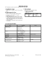
Page 6: ...LGE Spec Storage Environment 1 Temp 20 60 deg 2 Humidity 85 1 Application range This specification is applied to the LCD TV used LB81A chassis 2 Requirement for Test Each part is tested as below without special appointment 1 Temperature 25 5ºC 77 9ºF CST 40 5ºC 2 Relative Humidity 65 10 3 Power Voltage Standard input voltage 100 240V 50 60Hz Standard Voltage of each products is marked by models 4 ...

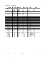
Page 7: ...1280 768 47 78 59 87 79 5 WXGA 6 1360 768 47 72 59 8 84 75 WXGA 7 1366 768 47 56 59 6 84 75 WXGA 5 Component Video Input Y PB PR No Specification Remark Resolution H freq kHz V freq Hz 1 720x480 15 73 59 94 SDTV DVD 480i 2 720x480 15 75 60 SDTV DVD 480i 3 720x480 31 47 59 94 SDTV 480p 4 720X480 31 5 60 SDTV 480p 5 720x576 15 625 50 SDTV DVD 576i 6 720x576 31 25 50 SDTV 576p 7 1280x720 44 96 59 94 ...

Page 8: ...94 27 00 SDTV 480P 4 3 2 720 480 31 50 60 27 027 SDTV 480P 4 3 3 640 480 31 469 59 94 25 175 SDTV 480P 4 3 4 640 480 31 469 60 00 25 20 SDTV 480P 4 3 5 720 480 31 47 59 94 27 000 SDTV 480P 16 9 6 720 480 31 50 60 00 27 027 SDTV 480P 16 9 7 720 576 31 25 50 00 27 000 SDTV 576P 8 1280 720 37 50 50 00 74 176 HDTV 720P HDCP 9 1280 720 44 96 59 94 74 176 HDTV 720P HDCP 10 1280 720 45 00 60 00 74 250 HD...

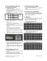
Page 9: ...ection 3 Main PCB check process APC After Manual Insult executing APC Download 1 Execute ISP program Mstar ISP Utility and then click Config tab 2 Set as below and then click Auto Detect and check OK message If display Error Check connect computer jig and set 3 Click Connect tab If display Can t Check connect computer jig and set 4 Click Read tab and then load download file XXXX bin by clicking Re...

Page 10: ...e by pushing ADJ key execute ADC Adjust by pushing G key at ADC CALIBRATION RGB PC 2 COMPONENT input ADC 1 Component Gain Offset Adjustment Convert to Component in Input source Signal equipment displays Impress Resolution 480i MODEL 209 in Pattern Generator 480i Mode Pattern 65 in Pattern Generator MSPG 925 Series MPSG 1025D 7 color bar Impress Resolution 1080i Model 223 in Pattern Generator 1080i...

Page 11: ...I1 2 3 4 and RGB because EDID data is in the Application Program 4 5 EDID DATA No USE the EDID data of Digital data HDMI 1 2 3 4 and Analog EDID data RGB As EDID data is recorded in the Mstar Main IC Except for RGB EDID data 1 ANALOG DATA 128Byte 2Bi Not USE EDID block 0 Bytes 0 127 00H 7FH Block Type EDID 1 3 2 DIGITAL DATA HDMI 1 256Byte Not USE EDID block 0 Bytes 0 127 00H 7FH Block Type EDID 1...

Page 12: ... 01 03 80 73 41 96 0A CF 74 A3 57 4C B0 23 20 09 48 4C A1 0C 00 31 40 45 40 61 40 81 80 D1 C0 30 01 01 01 01 01 01 02 3A 80 18 71 38 2D 40 58 2C 40 45 00 C4 8E 21 00 00 1E 01 1D 00 BC 52 D0 1E 20 50 B8 28 55 40 C4 8E 21 00 00 1E 00 00 00 FD 00 30 60 58 1F 64 11 00 0A 20 20 20 20 20 20 00 00 00 FC 70 00 4C 47 20 54 56 0A 20 20 20 20 20 20 20 01 6B 0 1 2 3 4 5 6 7 8 9 A B C D E F 0 02 03 23 F1 4E 93...

Page 13: ...NIT E4 00 00 EEPROM All clear EEPROM Read E7 00 00 EEPROM Read EEPROM Write E8 00 data EEPROM Write by some values COLOR SAVE EB 00 00 Color Save R G B cutoff Drive Contrast Bright H POSITION 20 00 00 64 They have different V POSITION 30 00 00 64 range each mode CLOCK 90 00 00 64 FOS Adjustment PHASE 92 00 00 64 R DRIVE 16 00 cool 00 80 Drive adjustment 01 medium 02 warm G DRIVE 18 00 cool 00 80 0...

Page 14: ...2 PROM 5 7 VRAM Read Send CMD 70h to read Video RAM value from MICOM And save its value to 128 Bytes Buffer Common Buffer for the use of EDID Delay 500ms Time to Wait and Read Video RAM from MICOM Be transmitted the contents of MICOM s 128 bytes Buffer to PC 128th Data is the CheckSum of 127 bytes data That s OK if the value of adding 128 bytes Data is Zero 14 LGE Internal Use Only Copyright 2008 ...

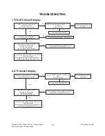
Page 15: ...t NO After checking the Power of Main IC IC100 you should decide to replace Main IC or not This board has big problem because Main IC IC100 have some troubles After checking thoroughly all path once again You should decide to replace Main Board or not Check the output data of TU401 Pin 24 34 Can you see the normal signal NO Could you measure voltage of TU800 IIC lines Are they all normal NO You sh...

Page 16: ...path once again You should decide to replace Main Board or not 4 Component doesn t display Check J701 Can you see the normal waveform Check the input of Component Audio switch IC1001 Can you see the normal waveform YES YES NO J701 may have problem Replace this Jack NO After checking the Power of component Audio switch you should decide to replace component Audio switch or not After checking the Po...

Page 17: ...B Audio switch or not NO After checking the Power of RGB Audio switch you should decide to replace RGB Audio switch or not Check the output of Main IC IC100 Especially you should check The H V sync and clock Can you see the normal waveform YES NO After checking the Power of Main IC IC100 you should decide to replace Main IC or not This board has big problem because Main IC IC100 have some troubles...

Page 18: ...and power of HDMI Switch you should decide to replace HDMI Switch or not NO NO After checking the Power of this chip you should decide to replace this or not After checking the Power of HDMI Switch you should decide to replace MST3361 or not YES Check HDCP communication lines IC902 NO After checking the Power of this chip you should decide to replace this or not Check the output of Main IC IC100 E...

Page 19: ... 35 OUT_N_L 29 IN_L 38 IN_R 5 HP_DET 37 MUTE 6 AUOUTR0 80 AUOUTL0 79 GPIO12 45 LVDS 177 190 194 199 RXE RXO BIN 1 SOGIN 2 GIN 3 RIN 4 VS_RGB 7 HS_RGB 8 SCL RX 33 SDA TX 34 DM_DET PB_IN 11 SOY 13 Y_IN 14 PR_IN 16 AUL_IN1 70 AUR_IN1 71 CVBS1 30 AUL_IN0 68 AUR_IN 69 SV_C0 25 SV_Y0 26 GPIO15 48 6612F00099A 0 27617 EAG31022001 0 185 Tx Rx IC603 MAX3232CDR Tx_Out Rx_In R232C_TXD R232C_RXD EEPROM AT24C02...

Page 20: ...TSVALID 104 IN 256 OUT 255 2 3 3V 1 8V HP_OUT_L 42 HP_OUT_R 1 OUT_P_R 8 OUT_N_R 14 OUT_P_L 35 OUT_N_L 29 IN_L 38 IN_R 5 HP_DET 37 MUTE 6 12V AUOUTR0 80 AUOUTL0 79 GPIO12 45 LVDS 177 190 194 199 RXE RXO BIN 1 SOGIN 2 GIN 3 RIN 4 VS_RGB 7 HS_RGB 8 SCL RX 33 SDA TX 34 DM_DET AUR_IN3 76 AUL_IN3 75 PB_IN 11 SOY 13 Y_IN 14 PR_IN 16 AUL_IN1 70 AUR_IN1 71 CVBS1 30 AUL_IN0 68 AUR_IN 69 SV_C0 25 SV_Y0 26 GP...

Page 21: ...trical and mechanical parts in this chassis have special safety related characteristics These parts are identified by in the Schematic Diagram and EXPLODED VIEW It is essential that these special safety parts should be replaced with the same components as recommended in this manual to prevent X RADIATION Shock Fire or other Hazards Do not modify the original design without permission of manufactur...

Page 22: ...Copyright 2008 LG Electronics Inc All right reserved Only for training and service purposes LGE Internal Use Only ...

Page 23: ...Copyright 2008 LG Electronics Inc All right reserved Only for training and service purposes LGE Internal Use Only ...

Page 24: ...Copyright 2008 LG Electronics Inc All right reserved Only for training and service purposes LGE Internal Use Only ...

Page 25: ...Copyright 2008 LG Electronics Inc All right reserved Only for training and service purposes LGE Internal Use Only ...

Page 26: ...Copyright 2008 LG Electronics Inc All right reserved Only for training and service purposes LGE Internal Use Only ...

Page 27: ...Copyright 2008 LG Electronics Inc All right reserved Only for training and service purposes LGE Internal Use Only ...

Page 28: ...Copyright 2008 LG Electronics Inc All right reserved Only for training and service purposes LGE Internal Use Only ...

Page 29: ...Copyright 2008 LG Electronics Inc All right reserved Only for training and service purposes LGE Internal Use Only ...

Page 30: ...Copyright 2008 LG Electronics Inc All right reserved Only for training and service purposes LGE Internal Use Only ...

Page 31: ...Copyright 2008 LG Electronics Inc All right reserved Only for training and service purposes LGE Internal Use Only ...

Page 32: ...Jun 2008 Printed in Korea P NO MFL42915904 ...

Reviews: