Lattice Semiconductor CrossLink Programming And Configuration Manual Download Page 16

CrossLink Programming and Configuration Usage Guide 


Technical Note  
 

© 2015-2017 Lattice Semiconductor Corp. All Lattice trademarks, registered trademarks, patents, and disclaimers are as listed at 

www.latticesemi.com/legal

All other brand or product names are 

trademarks or registered trademarks of their respective holders. The specifications and information herein are subject to change without notice. 

16 


FPGA-TN-02014-1.2 

5.


Configuration Modes 

CrossLink provides multiple options for loading the configuration SRAM from a non-volatile memory. The previous 
section describes the physical interface necessary to interact with the CrossLink Configuration Logic. This section 
describes the functionality of each of the different configuration modes. Descriptions of important settings required in 
the Diamond Spreadsheet View are also discussed. See th

Configuration

 section on page 9 for details on the default 

configuration behavior of the device. 

5.1.


SDM Mode 

SDM (Self-Download Mode) is the primary configuration method for CrossLink. The advantages of SDM include: 


Speed

: CrossLink is ready to run in a few milliseconds depending on the density of the device. 


Security

: The configuration data is never seen outside the device during the load to SRAM. You can prevent the 

internal memory from being read. 


Reduced cost

: There is no need to purchase a PROM specifically reserved for programming CrossLink. 


Reduced board space

: Elimination of an external PROM allows your board to be smaller. 

CrossLink retrieves the configuration data from the internal NVCM when it is using Self Download Mode. SDM is 
triggered when power is applied, a REFRESH command is received, or by asserting the CRESETB pin from HIGH to LOW. 

5.2.


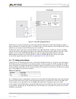
Master SPI Configuration Mode 

Master SPI (MSPI) configuration mode is the only other self-controlled configuration mode available to CrossLink. 
Lattice recommends having a secondary configuration port available that is active when CrossLink is in Feature Row 
HW Default Mode state (that is, blank). The secondary port allows you to recover CrossLink in the event of a 
programming error. 

For CrossLink to operate correctly using the MSPI configuration mode, ensure that: 


The POR of the SPI Flash device is lower than the POR of CrossLink or the SPI Flash is powered first. 


SPI Flash Fmax is greater than CrossLink MCK Fmax. 


Board routing requirements are checked to ensure CrossLink setup and hold time parameters are met. Refer to the 

CrossLink Family Data Sheet (FPGA-DS-02007) 

for detailed setup and hold time information. 

Table 5.1. Master SPI Configuration Port Pins 

Pin Name 

Function 

MCK 

Clock output from the CrossLink Configuration Logic and Master SPI controller. Connect MLK to the SCLK input 
of the Slave SPI device. 

MOSI 

Serial Data output from CrossLink to the slave SPI SI input. 

MISO 

Serial Data input to the CrossLink Configuration Logic from the slave SPI SO output. 

CSN 

Chip select output from the CrossLink Configuration Logic to the slave SPI Flash holding configuration data for 
CrossLink. 


Table 4.2

 provides information about the amount of memory needed for CrossLink configuration data by device 

density. Select an SPI Flash that accepts 03 hex Read Opcodes. CrossLink is only able to use the 03 hex Read Opcode. 

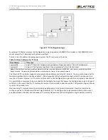
CrossLink begins retrieving configuration data from the SPI Flash when power is applied, a REFRESH command is 
received, or the CRESETB pin’s LOW to HIGH transition which puts the FPGA into Master SPI configuration mode. The 
MCK/SPI_SCK I/O takes on the Master Clock (MCK) function, and begins driving a nominal 2 MHz clock to the SPI Flash’s 
SCLK input. CSSPIN is asserted LOW, commands are transmitted to the PROM over the MOSI output, and data is read 
from the PROM on the MISO input pin. When all of the configuration data is retrieved from the PROM, the CSSPIN pin 
is deasserted and the MSPI output pins are tri-stated. 

The MCK frequency always starts downloading the configuration data at the nominal 2 MHz frequency. The 
MCCLK_FREQ parameter, accessed using Spreadsheet View, can be used to increase the configuration frequency.  

The configuration data in the PROM has some padding bits, and then the data altering the MCK base frequency is read. 
CrossLink reads the remaining configuration data bytes using the new MCK frequency. 

Summary of Contents for CrossLink

Page 1: ...CrossLink Programming and Configuration Usage Guide Technical Note FPGA TN 02014 Version 1 2 December 2017...

Page 2: ...s Default Behavior and Arbitration 8 4 4 Configuration 9 4 5 Wake up 9 4 6 User Mode 9 4 7 Clearing the Configuration Memory and Re initialization 10 4 8 Bitstream PROM Sizes 10 4 9 Configuration Mode...

Page 3: ...Figure 5 2 I2 C Configuration Logic 20 Figure 5 3 Bitstream Update Using TransFR 21 Figure 5 4 Example Process Flow 22 Figure 6 1 sysCONFIG Preferences in Global Preferences Tab Diamond Spreadsheet Vi...

Page 4: ...The specifications and information herein are subject to change without notice 4 FPGA TN 02014 1 2 Acronyms in This Document A list of acronyms used in this document Acronym Definition CRC Cyclic Red...

Page 5: ...an internal Non Volatile Configuration Memory NVCM as well as flexible SPI and I2 C configuration modes CrossLink provides a rich set of features for the programming and configuration of the FPGA Many...

Page 6: ...the configuration data from the non volatile memory Dummy Byte A dummy byte is any data in which the numeric value is considered to be invalid In some cases external devices controlling the resident...

Page 7: ...Flow Before it is operational the FPGA goes through a sequence of states including initialization configuration and wake up Figure 4 1 shows the configuration flow Figure 4 1 Configuration Flow The Cr...

Page 8: ...ring power up or when CRESETB pin toggles from LOW to HIGH or REFRESH command execution the Configuration Logic puts the device into master auto boot mode The device boots either from internal NVCM or...

Page 9: ...eived the FPGA asserts an internal DONE status bit The assertion of the internal DONE causes a Wake up state machine to run that sequences four controls The four control strobes are External CDONE Glo...

Page 10: ...mory must be loaded with valid configuration data before the FPGA operates CrossLink provides four modes of loading the configuration data into the SRAM memory The four modes available are Self Downlo...

Page 11: ...r Mode Table 4 4 Default State in Diamond for each Port sysConfig Port Diamond Default1 CDONE_PORT CDONE_USER_IO SLAVE_SPI_PORT Enable I2C_PORT Disable MASTER_SPI_PORT Disable2 Note 1 This default set...

Page 12: ...ternal DONE bit defines the beginning of the FPGA Wake up state The CDONE output pin is controlled by the CDONE_PORT and DONE_EX configuration parameter that is modified in the Diamond Spreadsheet Vie...

Page 13: ...Configuration Logic MISO SO Output This is the output from the slave which carries output data from the CrossLink Configuration Logic to the external SPI master SPI_SS SPI_SS Input with weak pullup Cr...

Page 14: ...MISO and MCK SPI_SS They are not permitted to be accessed at the same time In Diamond if both the ports are enabled at the same time the flow fails SPI_SS must be deasserted even if recovered for GPIO...

Page 15: ...iguration sequence at the Initialization phase as described in this Tech Note Holding the CRESETB pin LOW prevents CrossLink from leaving the Initialization phase An external SPI Master can also write...

Page 16: ...you to recover CrossLink in the event of a programming error For CrossLink to operate correctly using the MSPI configuration mode ensure that The POR of the SPI Flash device is lower than the POR of...

Page 17: ...tored in external SPI Flash or NVCM If the primary image configuration fails CrossLink attempts to configure itself using a failsafe golden image stored in either external SPI Flash or NVCM The load o...

Page 18: ...the external SPI Flash 3 Refresh or power cycle Option B Using offline mode to program external SPI Flash 1 Program the external SPI Flash first may be none background mode 2 Program CrossLink interna...

Page 19: ...ode as per the user specific environment programming master refer to the Programming Tools User Guide document 5 5 I2 C Configuration Mode CrossLink has an I2 C Configuration port for use in accessing...

Page 20: ...sses Note Although there are four possible combinations of the reserved address bits 1000 0XX only the two combinations listed above are used The remaining two addresses are reserved for future I2C bu...

Page 21: ...ther Lattice FPGAs provides for the TransFR capability TransFR is described in Minimizing System Interruption During Configuration Using TransFR Technology TN1087 Figure 5 3 is an example of how you c...

Page 22: ...t is triggered during device wake up after Refresh instruction is issued attention needs to be given in designing I O with following conditions Register output pins Impact on the system board level wh...

Page 23: ...As provide dedicated I O pins to select the configuration mode CrossLink uses the non volatile Feature Row to select how it will configure The Feature Row s default state needs to be modified in almos...

Page 24: ...ents you from over assigning I O to the port pins DISABLE This setting disconnects the SPI port pins from the Configuration Logic By itself it does not make the port pins general purpose I O Both SLAV...

Page 25: ...default mode for building configuration data The configuration bitstream is stored in the Configuration NVCM NVCM EXT This setting boots up the system using the NVCM first If an error occurs the syste...

Page 26: ...t receives the configuration data using a USERCODE receives the same USERCODE value The TraceID is 64 bits long with the least significant 56 bits being immutable data The 56 bits are a combination of...

Page 27: ...uration is completed the SRAM is loaded the device wakes up in a predictable fashion If the CrossLink device is the only or the last device in the chain the Wake up process begins when configuration i...

Page 28: ...hange Summary December 2017 1 2 Updated the Configuration Process and Flow section Removed references to Table 4 1 Updated the Power up Sequence section Added information on upstream sources Changed V...

Page 29: ...e Version Change Summary February 2017 1 1 Updated the Configuration Ports Default Behavior and Arbitration section with default behavior Updated the Configuration section with two cases Added Note 2...

Page 30: ...7th Floor 111 SW 5th Avenue Portland OR 97204 USA T 503 268 8000 www latticesemi com...

Reviews: