background image

20


www.lairdtech.com


Laird Technologies


BTM510/511

Bluetooth

® 

Multimedia Module

CONFIgurINg  

THE BTM510/511

REGISTER

DEFAULT

RANGE

COMMENT

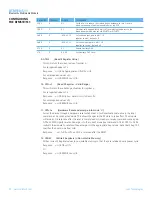
S592

0

0..1

Set this to 1 to reduce the trusted device database to just 1 record  
when autosaving of pairing is enabled via S reg 538

S593

0

0..1

Automatically append last 6 digits of local bluetooth address to the  
friendlyname which was set via AT+BTN or AT+BTF

S689

0

-450..+215

Set codec output gain in dBr * 10
(applies to sink), default = 0

S690

0

-450..+215

Set codec input gain in dBr * 10
(applies to source), default = 0

S730

0

0..1

Enable Auxiliary DAC

S731

0

0..225

Set Auxiliary DAC Level


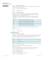
9. ATSn?        {Read S Register Value}


  This will return the current value of register n.


  For recognised values of n


  Response:  <cr,lf>As Appropriate<cr,lf>OK<cr,lf>


  For unrecognised values of n


  Response:  <cr,lf>ERROR nn<cr,lf>


10. ATSn=?        {Read S Register – Valid Range}


  This will return the valid range of values for register n.


  For recognised values of n


  Response:  <cr,lf>Sn:(nnnn..mmmm)<cr,lf>OK<cr,lf>


  For unrecognised values of n


  Response:  <cr,lf>ERROR nn<cr,lf>


11. ATZ<n>        {Hardware Reset and emerge into mode ‘n’}


  Forces the device through a hardware reset which means it will eventually come alive in the local  


  command and unconnected mode. This allows changes to the PS store to take effect. The module  


  will issue an OK response after the reset is complete and it is ready to receive commands once again.


  ATZ and ATZ0 signify reset and emerge into the current mode (see command ATI14). ATZ1 to ATZ4  


  instructs the module to reset and then emerge into the appropriate boot mode. Note that S Reg 103  


  specifies the boot mode from cold.


  Response:       <cr,lf>OK<cr,lf> and OK is returned after the RESET


12. AT&W        {Write S Registers to Non-volatile Memory}


  Writes current S Register values to non-volatile memory so that they are retained over a power cycle.


  Response:  <cr,lf>OK<cr,lf>


  Or


  Response:  <cr,lf>ERROR nn<cr,lf>

Summary of Contents for BTM511

Page 1: ...BTM510 511 MULTIMEDIA MODULE USER MANUAL Innovative Technology for a Connected World www lairdtech com ...

Page 2: ... the BTM510 511 9 References 9 Glossary of Terms 10 AT Command Set 11 Assumptions 11 Commands 11 General AT Commands 11 General Bluetooth Control 22 Hardware Unit Control 28 Bluetooth Profiles 30 Secure Simple Pairing 37 Link Key Management 37 Miscellaneous 38 Appendix 39 BT MM Unsolicited Messages 39 BT MM Error Responses 39 Mechanical Drawings 41 Mechanical Details 41 Recommended PCB Footprint 4...

Page 3: ...f flash memory in the module allows complex functionality to be included DSP routines can be licensed through a number of specialist partners Typical applications for these modules include Bluetooth stereo headsets VoIP phones and wireless audio links To speed product development and integration Laird Technologies has developed a comprehensive AT command interface that simplifies application devel...

Page 4: ... RS 232 bi directional for commands and data 16550 compat ible Baud Rate Configurable from 1 200 to 921 600bps Non standard baud rates supported Bits 8 Parity Odd even none Stop bits 1 or 2 Default Serial parameters 9 600 n 8 1 Levels Set by VDD_USB pin Modem Control DTR DSR DCD RI RTS CTS General Purpose Interface I O 8 general purpose I O pins I2 S Stereo Audio Digital Interface Bus LED Two Audi...

Page 5: ...n 1 5mA Supply Voltage Supply 3 0V 3 6V DC I O 1 7V 3 6V DC USB 1 7V 3 6V DC Coexistence Compatibility WLAN 802 11 2 wire and 3 wire hardware coexistence schemes supported Connections External Antenna option Pad for 50 Ohm antenna BTM510 Interface Surface Mount Pads Physical Dimensions 14 0mm x 20 0 x 1 6mm BTM510 14 0mm x 26 0mm x 1 6mm BTM511 provisional Weight 3 grams Environmental Operating Te...

Page 6: ...IO 22 GND 23 AUDIO_GND Audio ground 24 SPKR_A_N Speaker channel A left See note 3 25 SPKR_A_P Speaker channel A left See note 3 26 SPKR_B_N Speaker channel B right See note 3 27 SPKR_B_P Speaker channel B right See note 3 28 MIC_BIAS Microphone bias See note 4 29 MIC_BP_C Microphone channel A left See note 4 30 MIC_BN_C Microphone channel A left See note 4 31 MIC_AP_C Microphone channel B right Se...

Page 7: ...H 15pF 15nH 15pF The input impedance on the microphone inputs in microphone mode is typically 6kΩ In order to maintain the regulation on the MIC_BIAS pin the current drawn must be in the range 0 2 1 23mA If the microphone draws less current than this then an additional resistor to ground must be added to pre load the microphone output The audio input is designed for use with inputs of between 1μA ...

Page 8: ...nditions Operating Condition Min Max VDD_USB USB compatibility not required 1 7 3 6 VDD_USB USB compatibility required 3 1 3 6 VDD_IO 1 7 3 3 VDD_IN 3 0 3 6 Voltage Specifications Logic Levels VUSB Input Voltage Levels Min Typ Max Vih 0 625VDD_USB VDD_USB 0 3 Vil 0 3 0 25VDD_USB Output Voltage Levels Voh Iout 4mA 0 75VDD_USB VDD_USB Vol Iout 4mA 0 0 125 Logic Levels VIO Input Voltage Levels Min Ty...

Page 9: ... or automatically connects The device has a serial interface and an RF communications end point The latter has a concept of connected and unconnected modes and the former will have a concept of command and data modes This leads to the matrix of states shown below RF Unconnected RF Connected Local Command Mode OK OK Remote Command Mode ILLEGAL OK Data Mode ILLEGAL OK The combinations Data and RF Un...

Page 10: ...an analogue digital signal DAC Digital to Analogue Converter DSP Digital Signal Processor DUN Dial Up Network Profile FTP File Transfer Profile GOEP Generic Object Access Exchange Profile GPIO General Purpose Input Output HFP Hands Free Profile HID Human Interface Device Profile I O IO Input Output Mic Microphone OPP Object Push Profile PBAP Phone Book Access Profile PWM Pulse Width Modulation Sxx...

Page 11: ... delimited by double quotes E g Hello World The character MUST be supplied as delimiters uuid A 4 character UUID number consisting of ASCII characters 0 to 9 A to F and a to f General AT Commands 1 AT Used to check the module is available Response cr lf OK cr lf 2 ATA Answer Call Accept an incoming connection which is indicated by the unsolicited string cr lf RING 123456789012 cr lf every second 1...

Page 12: ...oth R and L modifiers are specified then an error will be returned Response cr lf CONNECT 123456789012 AE cr lf Or cr lf NO CARRIER cr lf 6 ATEn Enable Disable Echo This command enables or disables the echo of characters to the screen A valid parameter value will be written to S Register 506 All other values of n will generate an error Response cr lf OK cr lf Or Response cr lf ERROR nn cr lf 7 ATH...

Page 13: ... of 0 disables this feature If S0 0 and S100 0 then S0 must be S100 If a value is entered which violates this rule then ERROR 29 is sent in response S101 1101 0 ffff UUID of default SPP based profile when not specified explicitly in the ATD command S102 1 1 0x7FF Defines a set of bits masks for enabling profile servers Values can be ORed 0x001 is Serial Port Profile 0x080 is A2DP 0x100 is AVRCP S1...

Page 14: ...adphone default Bit 1 Speaker Bit 2 Recorder Bit 3 Amplifier S313 1 0 15 A2DP source supported features Bitmask Bit 0 Player default Bit 1 Microphone Bit 2 Tuner Bit 3 Mixer S320 2 1 3 Security Level see 12 Generic Access Profile Table 5 7 needs subsequent AT W and power cycle to take effect S321 1 0 4 Set IO capability 0 display only 1 display yes no 2 keyboard only 3 no input no output 4 reject ...

Page 15: ...before abandoning connection attempt as a master Referenced by ATD In units of seconds See S Registers 530 and 543 also Please note that as disconnection time can vary this register only guarantees the minimum delay Note that for invalid addresses specified in the ATD command the NO CARRIER response will be immediate See S register 560 for specifying disconnect max timeout S506 1 0 1 Enable Disabl...

Page 16: ...serted then S Reg 567 S514 10 1 60 Pairing Timeout in seconds This includes the time a host takes to supply the PIN number when PIN messages are indicated S515 0x001F00 0 0xFFFFFF Default Device Class Code on power up When queried the value is always printed as a hexadecimal number To change the device class of the module permanently use this S register plus subsequent AT W and ATZ To change the d...

Page 17: ...onnectable or discoverable then GPIO4 will blink This register will not necessarily be effective immediately after changing the value It must be saved to non volatile store using AT W and will operate as expected after an ATZ or a power cycle S535 20 0 41 Link Supervision Timeout If units go out of range then a NO CARRIER message will be sent to the host after the time specified here S536 0 0 1 Wh...

Page 18: ...e in command and connected mode then on going back online using the ATO command a fresh signal will be sent to the peer to update the bits S552 0x0122 0x0FFF This register specifies in each 4 bit nibble how the DTR DCD RI output pins are controlled when in a Bluetooth connection Nibble 0 3 specifies the source for DTR 4 7 specifies the source for DCD 8 11 specifies the source for RI Each nibble ca...

Page 19: ...k When Bit 1 is 1 then error responses do not include the error number and instead the error number can be retrieved using ATI12 S560 15 15 120 Disconnect timeout in seconds This timer specifies how long to wait for confirmation from the peer device and or the underlying stack that the connection has been successfully torn down There can be instances where a confirmation does not arrive and so in ...

Page 20: ... S Register Valid Range This will return the valid range of values for register n For recognised values of n Response cr lf Sn nnnn mmmm cr lf OK cr lf For unrecognised values of n Response cr lf ERROR nn cr lf 11 ATZ n Hardware Reset and emerge into mode n Forces the device through a hardware reset which means it will eventually come alive in the local command and unconnected mode This allows cha...

Page 21: ...ipset I8 The chipset format I9 0 if not in a connect state and 1 if in a connect state I11 The reason why a NO CARRIER resulted in the most recent attempt at making an outgoing connection Where the response values are as follows 0 No prior connection 1 Connection timeout 2 Connection attempt cancelled 3 Normal disconnection 4 Peer device has refused connection 5 Service profile uuid requested not ...

Page 22: ...ve and assuming the peer device is also a Laird Technologies device this command is used to start stop a SCO channel to transfer audio between the two peer devices The value N is a bit mask indicating the packet type to be used on the SCO link If n is set to 0 the SCO channel is disabled On receipt of the command the following response immediately follows Response cr lf OK cr lf The lower layers t...

Page 23: ... the device is not in the database then the response will still be an OK Response cr lf OK cr lf 5 AT BTD Remove All Trusted Devices This command is used to remove all devices from the list of trusted devices in the non volatile database No confirmation will be asked for So beware WARNING If you make an authenticated connection the link key gets cached in the underlying stack So if you subsequentl...

Page 24: ...used to filter inquiry responses When devclass is 2 hexadecimal characters long it forces the inquiry to filter responses to devices that match their major device class code to this value which can only be in the range 00 to 1F Response cr lf 12346789012 cr lf 12345678914 cr lf OK cr lf If the module is waiting for an incoming connection entered via AT BTP AT BTG AT BTQ then it will respond with E...

Page 25: ... empty string deletes the key from the non volatile memory The string length must be in the range 0 to 8 otherwise an error will be returned Response cr lf OK cr lf 14 AT BTM bd_addr Set Incoming Peer Address This command is used to set the peer address Response cr lf OK cr lf 15 AT BTM Delete Incoming Peer Address This command is used to delete the peer address previously stored using AT BTM bd_a...

Page 26: ...ss specified In this circumstance all commands from the host are buffered in the receive buffer until a Bluetooth connection is established with the peer device and it then sends the buffer across This means that if the peer device is not in the vicinity and will never be there the device effectively becomes useless as in this circumstance a host would want to get attention of the AT parser to sen...

Page 27: ...e the AT BTK command For a successful pairing the link key is stored in a volatile cache which is overwritten every time a new pairing is initiated using this command The link key can be stored in a non volatile database within the device The list of trusted devices is managed using commands AT BTT AT BTT and AT BTD The AT BTT command produces a list of trusted Bluetooth addresses link key is NEVE...

Page 28: ...689 and S690 the overall gain dBr must be entered multiplied by 10 If the input value doesn t match a gain table entry the nearest possible value is set The actually set value can be checked by reading back S689 S690 The value of S689 S690 is printed out multiplied by 10 in order to avoid non integer numbers The command class AT G allows incremental decremental control of codec gain settings The i...

Page 29: ...15 See Gain Table S690 is affected too Set input overall gain dBr S690 450 215 default 0 See GainTable value must be entered and is returned multiplied by 10 S590 is affected too Increment current output gain level AT GOU Error 57 may appear if maximum gain level reached Decrement current output gain level AT GOD Error 58 may appear if minimum gain level reached Query current output gain level AT ...

Page 30: ...vated by setting the appropriate Flag in S Register 102 see Table 3 1 After S Register 102 has been written all S Registers must be saved to non volatile memory AT W and subsequently a reset has to be carried out ATZ 2 A2DP The Advanced Audio Distribution Profile is used to transmit high quality audio streams between two Bluetooth devices An A2DP role must be assigned to a BT MM module either sour...

Page 31: ...450 215 Set codec input gain in dBr 10 applies to source default 0 Set A2DP sink supported features bit mask S312 0 15 Bitmask sink supported features Bit 0 Headphone default Bit 1 Speaker Bit 2 Recorder Bit 3 Amplifier Set A2DP source supported features bit mask S313 0 15 Bitmask source supported features Bit 0 Player default Bit 1 Microphone Bit 2 Tuner Bit 3 Mixer 3 AVRCP The Audio Video Remote...

Page 32: ...command mode S Register 531 is ignored for AVRCP connections 3 1 2 Release AVRCP control connection AT AVH Release AVRCP control connection Response cr lf NO CARRIER 110E cr lf 3 1 3 Send UNIT INFO Request AT AVU Send a Unit Info request to a connected AVRCP target Response immediately cr lf OK cr lf On command completion cr lf AVUR n unit_idhex unit_typehex company_idhex cr lf n statusdec 0 succe...

Page 33: ...lf AVPTC n operation_idhex button_state cr lf after command completion If status n indicates an unsuccessful outcome operation_idhex and button_state are omitted 3 2 AVRCP Target TG This section describes AT Commands and S registers when BT MM is configured as an AVRCP Target S301 2 In this mode BT MM supports one subunit PANEL see 5 3 2 1 Incoming AVRCP Connection Request An incoming AVRCP connec...

Page 34: ... S305 0 1 default 1 Enable Subunit Info Response S306 0 1 default 1 Configure PASS THROUGH PT Response S310 0 1 1 Enable automatic PT response response type is read from S311 default 0 Host is required to respond to PT Indication see AT PTR Set automatic response type S311 0 7 This value is queried for automatic PT Response see Table 3 10 Default value is accepted 1w 9r Advertise service S102 256 ...

Page 35: ...B Favourite menu 0x0C Exit 0x0D 0 0x20 1 0x21 2 0x22 3 0x23 4 0x24 5 0x25 6 0x26 7 0x27 8 0x28 9 0x29 Dot 0x2A Enter 0x2B Clear 0x2C Channel up 0x30 Channel down 0x31 Sound select 0x32 Input select 0x33 Display information 0x34 Help 0x35 Page up 0x36 Page down 0x37 Power 0x40 Volume up 0x41 Volume down 0x42 Mute 0x43 Play 0x44 PLAY Stop 0x45 STOP Pause 0x46 PAUSE Record 0x47 Rewind 0x48 REWIND Fas...

Page 36: ... Message Comment CONNECT 123456789012 110E AVRCP control connection established 123456789012 bd_addr of peer device 110E UUID indicating AVRCP NO CARRIER 110E AVRCP connection rejected or closed NO CARRIER All Connections closed AVUR n unit_idhex unit_typehex company_idhex AV Unit Info Response sent in response to AT AVU UNIT INFO Request n statusdec 0 success 1 Fail 2 Timeout unit_idhex Unit ID u...

Page 37: ... specification general bonding is defined as the exchange of link keys between two devices with the intention of establishing a connection immediately This is the case if a device wants to connection to another device without existing link key Hence pairing authentication and exchange of link keys is initiated automatically prior to the connection General bonding is initiated by ATD BdAddr AT APD ...

Page 38: ...released ATH may be used Please see Table 3 13 3 Production Info String A string with production information can be retrieved by ATI200 Table 3 13 Profile Release Commands Task AT Command Comment Disconnect A2DP ATH110D orAT APH If A2DP connection released response NO CARRIER 110D If no A2DP connection has existed response NO CARRIER Disconnect AVRCP ATH110E or AT AVH If AVRCP connection released ...

Page 39: ...ex button_state subunit_idhex subunit_typehex Indication of incoming Pass Through command operation_idhex see Table 3 8 button_state 0 pushed 1 released subunit_idhex subunit id subunit_typehex subunit type see Table 3 9 AVPTC n operation_idhex state Confirmation of AT AVC Control Command Request n 0 successful 1 timeout 2 not successful other than timeout PAIR BdAddr Incoming pairing request from...

Page 40: ...er cannot be specified in ATD command 35 Invalid Major Device Class valid value in range 0x00 to 0x1F inclusive 36 Pairing in progress Command cannot be actioned try again later 37 Invalid Sniff parameter specified E g new Attempt value greater than MinInterval Solution is to first increase MinInterval and re enter the Attempt value 38 Get Remote Friendly name Failed 39 Failed to change mode to Mu...

Page 41: ...50 G 3 00 PCB Thickness RF Shield Height Global pad width Global pitch 2 3 H 0 85 Global length of pad to edge of board Units mm Pin Outs RF Shield U1 U3 Orientation mark on PCB and RF Shield denotes pin 1 F H 1 3 0 65 0 55 Pad Centre to Board edge Pad Centre to Board edge 1 12 13 27 28 54 40 39 1 12 13 27 28 54 40 39 TOP VIEW BOTTOM VIEW COMPONENT SIDE SMT PADS E D 34 34 RF OUT RF OUT SIDE VIEW D...

Page 42: ...R16 0R 1 2 R25 NF 0R R25 NF 0R 1 2 R2 0R R2 0R 1 2 C33 NF 100u C33 NF 100u R22 NF 0R R22 NF 0R 1 2 J2 3 way 2 5mm audio jack J2 3 way 2 5mm audio jack 1 2 4 3 C3 100u C3 100u 1 2 SW3 NF SW3 NF 1 3 2 4 R17 0R R17 0R 1 2 C14 15pF C14 15pF 1 2 R10 1MR R10 1MR 1 2 R15 0R R15 0R 1 2 R6 0R R6 0R 1 2 SW4 NF SW4 NF 1 3 2 4 TP3 TP3 1 C12 15pF C12 15pF 1 2 R9 39R R9 39R 1 2 R29 0R R29 0R 1 2 R36 2K2 R36 2K2...

Page 43: ...GND 3 OUT 4 VCC 5 U4 CONN_SM_54 U4 CONN_SM_54 PIO_15 DTR 1 PIO_5 BT_STATE BT_PRIORITY 2 PCM_IN 3 PCM_OUT 4 PCM_SYNC 5 PCM_CLK 6 VDD_USB 10 VDD_IO 11 MASTER_VIN 12 SPI_CS 14 SPI_MISO 15 SPI_CLK 16 SPI_MOSI 17 PIO_2 DSR 18 LED_EXT1 7 LED_EXT0 8 PIO_0 BT_ACTIVE 21 GND2 22 AUDIO_GND 23 SPKR_A_N 24 SPKR_A_P 25 SPKR_B_N 26 SPKR_B_P 27 MIC_BIAS 28 BC05_RST 54 PIO_6 WLAN_ACTIVE 53 USB_D 46 USB_D 45 PIO_7 ...

Page 44: ...M1 Mounting Hole R84 10K R84 10K 1 2 R73 110R R73 110R 1 2 R90 0R R90 0R 1 2 L5 BLM18PG221SN1D L5 BLM18PG221SN1D 1 2 FID2 Fiducial FID2 Fiducial D3 Diode_S1A D3 Diode_S1A 1 2 R11 NF 9K1 R11 NF 9K1 1 2 CN1 DC Power jack_2 1mm CN1 DC Power jack_2 1mm 1 2 3 R77 1K R77 1K 1 2 R91 NF 9K1 R91 NF 9K1 1 2 R81 0R R81 0R 1 2 U6 MCP1726 ADJE MF U6 MCP1726 ADJE MF Vin_1 1 Vin_2 2 SHDN 3 GND 4 PWRGD 5 Cdelay 6...

Page 45: ...enna Q2 2009 DVK BTM510 Development Board with BTM510 soldered in place Q1 2009 DVK BTM511 Development Board with BTM511 soldered in place Q2 2009 General Comments This is a preliminary datasheet Please check with Laird Technologies for the latest information before commencing a design If in doubt ask Refer to the schematic BTV R 003 pdf for the Development Kit on the following two pages for examp...

Page 46: ...ress statutory and implied or by description regarding the information set forth herein Laird Technologies reserves the right to change specifications at any time and without notice Laird Technologies products are intended for use in normal commercial and industrial applications Applications requiring unusual environmental requirements such as military medical life support or life sustaining equip...

Reviews: