14
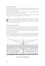
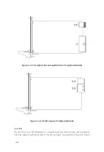
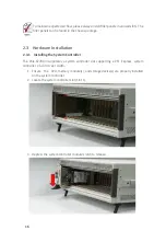
The solid circle shown represents the source of the trigger and the transparent
circle the trigger destination.
For details regarding configuration of trigger bus bridge routing please see “Trigger Bus”
on page 25.
Reference Clock
The PXIe-62780 backplane supplies a single-ended 10MHz reference clock (PXI_CLK10)
and differential 100MHz clock (PXIe_CLK100) to each peripheral slot for inter-module
synchronization. The independent buffers drive the clock signal to each peripheral slot.
These common reference clock signals can synchronize multiple modules in a PXI Express
chassis. PXI modules with phase-lock loop circuits can lock reference clocks to generate
an in-phase timebase.
The PXI_CLK10 and PXIe_CLK100 clocks are in-phase according to the PXI-5™
specification. Since the external 10MHz clock input can override the onboard 10MHz
clock source, a phase-lock loop (PLL) circuit on the backplane synchronizes the PXIe_
CLK100 and external 10MHz clock.
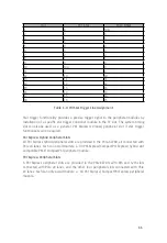
The PXIe-62780 PXI chassis automatically selects the 10 MHz reference clock source from
among:
• Built-in accurate 10 MHz clock source
• External 10 MHz clock through a BNC connector
• PXI_CLK10_IN pin on the system timing slot Priority of the 10MHz reference clock
is as follows.
System Timing Slot
(10th slot)
BNC Connector on Rear
Panel
10mhz Clock Driven to
Peripheral
Slots
No clock present
No clock present
10MHz clock is generated by
backplane
No clock present
10MHz clock present
Clock from BNC connector is
driven to all peripheral slots
10MHz clock present
No clock present
Clock from system timing slot is
driven to all peripheral slots
10MHz clock present
10MHz clock present
Clock from system timing slot is
driven to all peripheral slots
Table 1-5: PXIe-62780 Reference Clock Priority

