background image

SERVICE MANUAL

No.20920

Mar. 2001

COPYRIGHT      2001 VICTOR COMPANY OF JAPAN, LTD.

MX-G70

COMPACT COMPONENT SYSTEM

MX-G70

Area Suffix

J
C

U.S.A.

Canada

Safety precautions
Important for laser products
Warnings and Cautions
Preventing static electricity
Importance administering
                       point on the safety
Disassembly method

1-2
1-3
1-3
1-4

1-5
1-6

Adjustment method
Flow of functional operation
                       until TOC read
Maintenance of laser pickup
Replacement of laser pickup
Description of major ICs  

1-26

1-30
1-31
1-31
1-32

Contents

PLAY & EXCHANGE

STANDBY/ON

CD-R

/RW  PLAYBACK

STANDBY

MX-G70

SP-MXG70

CA-MXG70

SP-MXG70

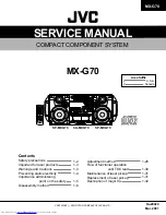
Summary of Contents for CA-MXG70

Page 1: ...nings and Cautions Preventing static electricity Importance administering point on the safety Disassembly method 1 2 1 3 1 3 1 4 1 5 1 6 Adjustment method Flow of functional operation until TOC read Maintenance of laser pickup Replacement of laser pickup Description of major ICs 1 26 1 30 1 31 1 31 1 32 Contents PLAY EXCHANGE STANDBY ON CD R RW PLAYBACK STANDBY MX G70 SP MXG70 CA MXG70 SP MXG70 ...

Page 2: ...rnet check Electrical shock hazard testing After re assembling the product always perform an isolation check on the exposed metal parts of the product antenna terminals knobs metal cabinet screw heads headphone jack control shafts etc to be sure the product is safe to operate without danger of electrical shock Do not use a line isolation transformer during this check Plug the AC line cord directly...

Page 3: ...ouch it in case of an adjustment or operation check CAUTION TO REDUCE THE RISK OF ELECTRIC SHOCK DO NOT REMOVE COVER OR BACK NO USER SERVICEABLE PARTS INSIDE REFER SERVICING TO QUALIFIED SERVICE PERSONNEL RISK OF ELECTRIC SHOCK DO NOT OPEN The lightning flash with arrowhead symbol within an equilateral triangle is intended to alert the user to the presence of uninsulated dangerous voltage within t...

Page 4: ...rce can easily destroy the laser diode 4 Handling the traverse unit optical pickup 1 Do not subject the traverse unit optical pickup to strong shocks as it is a sensitive complex unit 2 Cut off the shorted part of the flexible cable using nippers etc after replacing the optical pickup For specific details refer to the replacement procedure in the text Remove the anti static pin when replacing the ...

Page 5: ... for F101 and F102 This symbol specifies type of fast operating fuse Precaution Pour eviter risques de feux remplacez le fusible de surete de F001 comme le meme type que 5A 125V et 6A 125V pour F101 et F102 Ce sont des fusibles suretes qui functionnes rapide Importance administering point on the safety F001 F101 F102 ...

Page 6: ...es of the body Remove the metal cover from the body by lifting the rear part of the cover 1 2 3 Disassembly method Main body Removing the metal cover See Fig 1 to 3 Do not break the front panel tab fitted to the metal cover CAUTION Fig 1 Fig 2 Fig 3 A A A Metal cover Metal cover B Metal cover B ...

Page 7: ...changer mechanism assembly Disconnect the card wires from connector CN870 CN871 and CN315 on the main board respectively Remove the tie band and disconnect the wire from connector CN703 on the amplifier board Disconnect the wire from connector CN220 on the transformer board 1 2 3 Removing the front panel assembly See Fig 6 to 10 To prevent damage to the CD fitting be sure to pull both the rear pan...

Page 8: ...body Release the two joints a on the lower right and left sides of the body using a screwdriver and remove the front panel assembly toward the front 4 5 Fig 8 Fig 9 Fig 10 E Bottom Front panel assembly Joint a Joint a Front panel assembly Front panel assembly ...

Page 9: ...hanger mechanism assembly Remove the screw G attaching the rear cover on the back of the body Push each tab of the four joints b in the direction of the arrow and release Remove the eleven screws F attaching the rear panel Release the joints c on each lower side of the rear panel using a screwdriver and remove the rear panel backward 1 2 3 4 Removing the rear cover rear panel See Fig 12 to 15 Note...

Page 10: ...N211 and CN212 on the main board from the regulator board 1 2 3 4 Removing the main board See Fig 16 and 17 Prior to performing the following procedure remove the metal cover the CD changer mechanism assembly and the rear panel Disconnect connector CN217 on the speaker board from the regulator board 1 Removing the speaker board See Fig 18 It is not necessary to remove the main board REFERENCE Fig ...

Page 11: ...tage board from the regulator board The heat sink and heat sink bracket will be detached at once Pull out the upper and lower heat sink brackets from the heat sink respectively Remove the four screws I attaching the amplifier board to the heat sink Remove the two screws J the board bracket and the voltage board 1 2 3 4 5 6 Removing the amplifier board voltage board heat sink See Fig 19 and 20 Fig ...

Page 12: ... from connector CN204 on the regulator board Remove the two screws L attaching the regulator board 1 2 Removing the regulator board See Fig 23 Prior to performing the following procedure remove the metal cover the CD changer mechanism assembly and the rear panel Disconnect the wire from connector CN250 on the transformer board Remove the tie band from the voltage board Move the power cord stopper ...

Page 13: ... O attaching the display system control board If necessary disconnect the wire from connector CN911 on the front side of the display system control board and unsolder FW915 If necessary remove the CD play board Fig 28 1 2 3 4 Removing the display system control board See Fig 25 to 27 Remove the three screws P attaching the CD eject board If necessary unsolder FW915 on the CD eject board 1 2 Removi...

Page 14: ...nel and remove the nut Pull out the surround mode knob and the surround woofer level knob toward the front Remove the twelve screws R attaching the operation switch board Release the wire clamp Remove the screw R attaching the earth terminal extending from the switch board Release each tab of the seven joints g retaining the operation switch board 1 2 3 4 Removing the operation switch board See Fi...

Page 15: ...Fig 4 By removing the pawl at the section d fixing the return spring dismount the return spring See Fig 4 Remove the three lock levers See Fig 4 10 11 Fig 1 Fig 2 Fig 3 Fig 4 1 Remove the metal cover 2 Remove the CD changer mechanism assembly 3 From bottom side the CD changer mechanism assembly remove the four screws A retaining the CD servo control board 4 Absorb the four soldered positions a of ...

Page 16: ...15 Manually turn the motor pulley in the clockwise direction until the lifter unit stopper is lowered from the section e of CD tray assembly See Fig 8 Pull out all of the three stages of CD tray assembly in the arrow direction f until these stages stop See Fig 6 At the position where the CD tray assembly has stopped pull out the CD tray assembly while pressing the two pawls g and g on the back sid...

Page 17: ...tion k By raising the CD loading mechanism assembly in the arrow direction l remove the assembly from the lifter unit Fig 10 Fig 12 Fig 11 Fig 13 Removing the CD pick unit See Fig 13 1 2 3 4 Move the cam gear in the arrow direction m Then the CD pickup unit will be moved in the arrow direction n According to the above step shift the CD pickup unit to the center position While pressing the stopper ...

Page 18: ...m gear q align the Paul r position of the drive unit to the notch position Fig 16 on the cam gear q Pull out the drive unit and cylinder gear See Fig 17 While turning the cam gear q align the Paul s position of the select lever to the notch position Fig 18 on the cam gear q Remove the four screws H retaining the cam unit cam gear q and cams R1 R2 assembly See Fig 18 Cam gear q Drive unit r G H J H...

Page 19: ... in the arrow direction remove the gear bracket See Fig 18 From the notch u section on the chassis assembly fixing the edge of gear bracket remove and take out the gear bracket See Fig 19 Remove the belts respectively from the right and left actuator motor pulleys and pulley gears See Fig 18 After turning over the chassis assembly remove the actuator motor while spreading the four pawls v fixing t...

Page 20: ...m gear q See Fig 22 1 2 3 4 Remove the slit washer fixing the cams R1 and R2 assembly By removing the two pawls w fixing the cam R1 separate R2 from R1 Remove the slit washer fixing the cam gear q Pull out the cam gear q from the C G base assembly Removing the C G base assembly See Fig 22 and 23 Remove the three screws J retaining the C G base assembly Fig 23 Slit washer Pawl Cam R2 Slit washer Ca...

Page 21: ...th screw retaining the playback head 7 Take out the playback head from the front of the head mount 8 The recording and eraser heads should also be removed similarly according to Steps 1 7 above Reassembling the playback recording and eraser heads See Fig 3 1 Reassemble the playback head from the front of the head mount to the position as shown in Fig 3 2 Fix the reversing azimuth screw 3 Set the s...

Page 22: ...ssembly See Fig 5 to 7 1 Remove the six screws B retaining capstan motor assembly See Fig 5 2 While raising the capstan motor remove the capstan belts A and B respectively from the motor pulley See Fig 6 Caution 1 Be sure to handle the capstan belts so carefully that these belts will not be stained by grease and other foreign matter Moreover these belts should be hand while referring to the capsta...

Page 23: ...fixing the capstan shafts R and L and pull out the flywheels R and L respectively from behind the cassette mechanism Removing the reel pulse board and solenoid See Fig 11 1 Remove the five pawls c d e f g retaining the reel pulse P C Board 2 From the surface of the reel pulse P C Board parts remove the two pawls h and i retaining the solenoid Capstan motor Joint bracket Flywheel R Flywheel L Flywh...

Page 24: ...procedure remove the side cover Pull out the saran net toward the front while disengaging the four joints a Remove the two screw cover and two screws C attaching the inner front cover 1 2 Removing the front cover See Fig 3 to 6 Attention which adheres to speaker box The speaker box of this model is a unit supply Therefore we do not supply it as individual parts though the method of disassembling t...

Page 25: ... the body Pull out the woofer speaker toward the front and disconnect the wire yellow and black blue and black from the two speaker terminals 1 2 Removing the woofer speaker See Fig 7 Prior to performing the following procedure remove the side cover and the front cover Remove the two screws G attaching the tweeter speaker on the back of the front cover 1 Removing the tweeter speaker See Fig 8 Fig ...

Page 26: ...actor 30 FM modulation frequency 400Hz Frequency displacement 22 5kHz Frequency Range AM 531kHz 1710kHz FM 87 5MHz 108MHz Standard measurement positions of volume and switch Power Standby Light STANDBY Indicator Sub woofer VOL Minimum Sound mode OFF Main VOL 0 Minimum Traverse mecha set position Disc 1 Precautions for measurement 1 Apply 30pF and 33kohm to the IF sweeper output side and 0 082 F an...

Page 27: ...tion Back side Cassette Mechanism Unit Section Head azimuth adjusting screw Forward side Head azimuth adjusting screw Reverse side Head azimuth adjusting screw Forward side Head azimuth adjusting screw Reverse side Playback head Playback recording and eraser heads or playback head Tape speed ADJ Bias ADJ L Bias ADJ R ...

Page 28: ...corder section Items Measurement conditions Measurement method Standard values Adjusting positions After setting to the double speed motor confirm that the frequency counter reading becomes 4 800 400 300Hz when the test tape VTT712 3kHz has been play back with the playback mechanism When the test tape VTT712 3kHz has been played back with the playback mechanism or recording and playback mechanism ...

Page 29: ...de Test tape AC 225 Measurement output terminal Both recording and headphone terminals Reference frequency 1kHz and 10kHz REF 20dB Test tape TYP AC 225 Measurement input terminal OSC IN AC 225 4 20 A Output deviation between 1kHz and 10kH 1dB 2dB LcH VR101 RcH VR201 LcH VR101 RcH VR201 Electrical performance Items Measurement conditions Measurement method Standard values Adjusting positions 1 With...

Page 30: ...Automatic measurement of TE amplitude and automatic tuning of TE balance 500mv div 2ms div Fig 1 Approx 3sec pin 25 of IC601 TE Approx 1 8V VREF Tracking error waveform at TOC reading Power ON Play Key Confirm that the Focus error S cuve signal at the pin28 of IC651 is approx 2Vp p Confirm that the signal from pin24 IC651 is 0V as a accelerated pulse during approx 400ms Confirm the waveform of the...

Page 31: ... of the laser diode has expired the following symptoms will appear 1 The level of RF output EFM output ampli tude of eye pattern will below Is the level of RFOUT under 1 25V 0 22Vp p Replace it NO YES O K 3 Semi fixed resistor on the APC PC board The semi fixed resistor on the APC printed circuit board which is attached to the pickup is used to adjust the laser power Since this adjustment should b...

Page 32: ...mplifier input R1 R2 I Playback amplifier input NF2 Playback amplifier negative feedback OUT2 Playback amplifier output EQ2 I Equalizer CTL2 I Pre Amplifier input switching time constant RIN2 I Recording amplifier input RNF2 I Recording amplifier negative feedback ROUT2 O Recording amplifier output O LC I ALC low cut LPF I ALC low pass filter GND I Vcc Power supply RF I Ripple filter EQCTL EQ cont...

Page 33: ...IN1 2 IN1 3 VEE 4 BA15218F XE IC652 BA15218N IC481 501 502 526 546 571 Dual op amp 1 Pin layout 2 Block diagram Q19 Q17 Q16 OTHER CH R9 R6 R8 R7 R5 R4 R3 R2 R1 D1 C1 Q18 Q13 Q11 Q8 Q5 Vcc VEE OUTPUT IN IN Q1 Q3 Q4 Q2 C2 Q9 Q6 Q7 Q10 Q12 Q14 Q15 Q114 ...

Page 34: ...W P B S W G R E C S W C O N T G N D V c c 1 2 3 4 5 6 7 8 9 10 GND OUT1 P1 VZ IN1 IN2 VCC1 VCC2 P2 OUT2 Input Output Mode IN1 IN2 OUT1 OUT2 Brake 0 0 0 0 1 0 1 0 0 1 0 1 1 1 0 0 CLOCKWISE COUNTER CLOCKWISE Brake LB1641 IC851 IC852 DC motor driver 1 Pin layout 2 Pin function ...

Page 35: ...al Output selection control terminal Output selection control terminal Output selection control terminal Output selection control terminal Non connect Non connect Connected to GND upon normal use Multi plexor output terminal Connect to GND I O O O O O No Symbol I O Function 2 Pin Function 1 Block Diagrams BA3835S IC812 SPI B P F 1 2 3 4 5 6 7 8 9 18 17 16 15 14 13 12 11 10 BIAS VREF REFERENCE CURR...

Page 36: ...PEN DRAIN 12BIT STRAGE RESISTER 12BIT SHIFT RESISTER 1 Terminal Layout 1 2 3 4 5 16 17 18 Vss DATA CLOCK LCK Q0 Q11 OE Vdd I I I O I Connect to GND Serial Data input Shift Clock of Data Latch Clock of Data Parallel Data Output Output Enable Power Supply Pin No Symbol I O Function Latch Data L H OUTPUT ON OFF 2 Pin Function BU2092 F IC811 PORT EXPANDER ...

Page 37: ... AM OSC REG AM RF AFC AM AGC O I O I I I AM Local oscillation Signal output This is a terminal of AM Local oscillation circuit Register value between pin 26 and pin28 desides the frequency width of the input signal AM RF signal input This is an output terminal of voltage for FM AFC This is an AGC voltage input terminal for AM O O I O AM detection output FM detection output Mpx input terminal O O I...

Page 38: ...ts ON OFF BTL AMP 1 input pin BTL AMP 1 input pin For gain adjustment BTL AMP 1 input pin Non inverting side BTL AMP 1 input pin Inverting side BTL AMP 2 input pin Inverting side BTL AMP 2 input pin Non inverting side BTL AMP 2 input pin For gain adjustment BTL AMP 2 input pin External transistor collector PNP connection 5V power supply output External transistor PNP base connection Reset output R...

Page 39: ...output port Input output port Data input output Function IF counter signal input IF signal output Not use AM Local OSC signal output FM Local OSC signal input Power suplly VDD 4 5 5 5V When power ON Reset circuit move PLL charge pump output H Local OSC frequency Height than Reference frequency L Low Agreement Height impedance Input for active lowpassfilter of PLL Output for active lowpassfilter of...

Page 40: ... TUNER data input SLC TUNER clock Not used Power supply 5V Oscillation terminal 8MHz Connect to GND Not used Connect to GND Connect to GND Key matrix input 1 4 SLC Key input 1 SLC Key input 2 Not used SPI Analog data input AD 5V VC3 Ready Micon reset Bass volume Bass volume AUX muting RDS Data Karaoke SPI A data SPI B data Remote control signal input SLC Photo A SLC Photo B Soundmode reverse RDS C...

Page 41: ...nt control signal output Tuner chip enable System mute Skip LED LED Control signal output CD1 LED Control signal output CD2 LED Control signal output CD3 Reverse skip Music scan input Tuner stereo indicator Backup mode detect Forward skip Rotary encoder VOL Rotary encoder VOL Soundmode foeward B for FL O O O O O O O I I I I I I I I Pin No Symbol I O Function Pin function 2 2 ...

Page 42: ...MLD MCLK MDATA DSL PLL VCO SUB CODE BUFFER SSEL SQCK SUBQ CLVS CRC BLKCK CLDCK SBCK SUBC DEMPH FLAG6 RESY EFM DEMODULATION SUBCODE DEMODULATION SYNC INTERPOLATION 16k SRAM CIRC ERROR CORRECTION DE INTERLEAVE LRCKIN MSEL BCLK SSEL SRDATAIN PSEL IOSEL DIGITAL DE EMPHSIS 8TIMES OVER SAMPLING DIGITAL FILTER 1bit DAC PWM LOGIC PWM R PWM L DIGITAL AUDIO INTERFACE CLV SERVO INTERPOLATION SOFT MUTING DIGI...

Page 43: ...Kick pulse output Tracking drive output Focus drive output Reference voltage input pin for D A output block TVD FOD FBA TBAL Focus Balance adjust signal output Tracking Balance adjust signal output Focus error signal input Analog input Tracking error signal input Analog input RF envelope signal input Analog input Vibration detect signal input H detect Off track signal input H off track Track cross...

Page 44: ... TR1 TR3 TR2 TR4 TR5 TR6 TR8 R8 C2 TR14 TR15 TR16 R14 R11 R13 R12 R10 R9 TR9 TR10 TR12 TR13 TR11 TR7 C1 D1 R6 R3 R4 R5 R7 13 11 14 15 9 8 12 5 6 7 10 2 R2 SUB STK402 050 IC602 Power amp 1 Pin layout 2 Block diagram 1 15 ...

Page 45: ...VOLUME TREBLE TREBLE MIDLE MIDLE SPEAKER ATT RIGHT SPEAKER ATT LEFT BASS BASS SUPPLY G G I C BUS DECODER LATCHES 2 0 30dB 2dB STEP INPUT MULTIPLEXER GAIN CSL DIG GND TREBLE R TREBLE L MIN L MOUT L BOUT L BIN L BOUT R BIN R MOUT R MIN R INR MUXOUTR INL SDA CRE Vs AGND ROUT LOUT R IN4 R IN3 R IN2 R IN1 L IN1 L IN2 L IN3 L IN4 MUXOUTL TDA7439 1 2 3 4 5 6 7 8 9 10 11 12 13 14 15 30 29 28 27 26 25 24 2...

Page 46: ...inted in Japan 200103 V VICTOR COMPANY OF JAPAN LIMITED AUDIO COMMUNICATION BUSINESS DIVISION PERSONAL MOBILE NETWORK BUSINESS UNIT 10 1 1chome Ohwatari machi Maebashi city 371 8543 Japan No 20920 MX G70 ...

Page 47: ...3MSW A C B D E F F T FM SM ARF TX CD OUT L CAM R CAM SW1 6 PICKUP TRACKING FOCUS FEED M MICOM IC 810 FL DISPLAY FL 801 CN880 CN870 CN911 FW901 FW915 FW915 KEY LED SEARCH KNOB LED MAIN VOL WOOFER VOL SOUND MODE KEY LED KEY1 11 CD1LED CD2LED CD3LED SEARCH R F KEY21 22 VOL KEY2 3 21 32 41 42 KCMND MSTAT KCLK MRDY MPX VOLDA VOKCK M M FMN 008 FMB 028 3 FM AM DIGITAL OUT TX SPINDLE M FMB 028 1 FMC 022 0...

Page 48: ...209 F001 CN250 C253 CN209 C251 D255 C250 R253 RY3 D256 C253 QQT0319 002 T3 15AL T2AL T3 15AL QGA3901C1 03 QGA3901C1 03 QQT0253 002 1SS133 QQT0319 002 1N4003 QJK015 071214 QGD2504C1 03Z QGD2504C1 03Z 2SC2785 QJK015 071214 QJK015 071214 3 3k T2AL 1SS133 0 0047 250 QGB2510K2 04 T4AL QQT0319 003 T4AL T4AL 2SC2235 6A 125V 5A 125V 6A 125V T3 15AL QGD2504C1 03Z T4AL T4AL QQT0319 003 QGD2504C1 03Z QJK015 ...

Page 49: ...0 R667 Q613 R793 R795 R796 Q791 Q792 QGB2510J1 14 QGB2510K2 14 QGA3901C1 07 QGB2510J1 09 QGB2510K2 10 QSK0109 001 QSK0109 001 QGB2510J1 10 KRA111M T 1 2SD2395 KTC3199 GL 1 2K 1 2K 200 200 330 MTZJ5 1B 330 KTC3199 GL 10K 0 33 KIA7812API KRC104M T 1 0 022 0 022 2 2 KIA7808API KIA7809API QQR0779 001Z QNZ0136 001Z 2 7K 0 01 0 022 2A02M 1 1 KTC3199 GL T 100 35 10K 1SS133 10K 4 7 1N4003S T5 1N4003S T5 0...

Page 50: ...T2 2200P 0 001 0 01 22K 100k 220k 4 7k 4 7k KRA102M T 33K QGF1205C1 10 QGF1205C1 17 8 2k QGF1205C1 17 30k 30k 100k 100P 1 50 470 10 22K 100 10 6 8K 10K 100 0 22 4 7 50 10K QRJ146J 4 7X 1SS133 T2 100P MTZJ5 1B T2 QGF1016F3 19 47 16 1k 1k 1k 220k 5 6k 1k 1k 10K 0 1MY 10K 0 1 220 10 QUM156 18DGZ4 15k QQR0779 001 100 6 3 2SC2785 FE T 10K 2SC2785 FE T 2SC3576 JVC T 220k 47 16 47 16 2SC2785 FE T 47k 100...

Page 51: ...S133 T2 1K KRA102M T 22 50 1K 1K 0 1MY BA3835S 0 1MY QQL29BJ 100Z QQL29BJ 100Z QQL29BJ 100Z QQL231K 220Y 22 50 MN101C35DEA 100K 0 22 50 10K KRC104M T KRC104M T 100K 100K 10K 0 22 50 680k 1K 1K 1K 1K 1K 1K 1K KRC102M T 0 001 33P 33P 2 2 50 MTZ6 2JC 1N4003S T5 100K 100K 0 1MY 1SS119 02 T2 MTZ6 2JC 1 5MY 470 6 3 1N4003S T5 100K 1SS119 02 T2 5 6K 100K 100K 2SD1991A RS T 0 01 100K 100K 100K 10K 10K 10K...

Page 52: ...7 D918 D920 R919 R920 C1022 C1023 VR901 R1071 R1070 C1065 C1067 R1067 R1066 C1063 R1061 C1062 C1061 R1065 R1064 C1064 R918 QUB220 15DMHP QUM027 18Z4Z4 0 01 222P 0 01 QUM027 13DGZ4 102P 0 01 QSW0911 001 MTZJ2 4B T2 MTZJ2 4B T2 10K 0 01 0 01 QSW0862 001 QNS0183 001 QUB220 15DMHP QQL231K 470Y QUB023 33DGZ4 QSW0912 001 0 01 QSW0911 001 0 01 20K 4 7k 4 7k QNS0184 001 QNS0184 001 2SD2144S VW T NJM4580L ...

Page 53: ... 0 022 1 2K 56P 0 022 0 022 LB1641 LB1641 NI 270K 220K 0 001 0 001 10 1K QGA2001C1 06 150 10K 1K MN662748RPM 39k 4 7 470P 12P QAX0413 001Z 12P NI 1K 0 1 25 0 1 25 1K BA15218F XE BA15218F XE 0 047 2K 6 8K 10 16 5 6K 10K 100 10K 820 820 220 10 100 220 0 0068 0 0068 NI NI 390P 1K QGF1016F3 19 NI 1K 10K 390P 10K 0 047 NI NI NI NI 150k 2SB1357 EF T 10K 1 2K 47 10 1K 390k 1K 1K 1K 1K 1K 22K 0 022 2200p ...

Page 54: ...113 R3112 C3344 R3114 C3304 C3342 C3104 SW316 SW305 SW304 SW303 SW306 R3369 SW302 AN7345K 2SB562 C 10 KRC104M T QUM154 10Z4Z4 820P 2SB562 C KTA1267 YG T BA3126N 22K 10K 560P 2SC2001 K MTZJ5 1B T2 10P MTZJ5 1B T2 QQR0621 001Z QGF1205F1 09 QGF1205F1 10 KRC107M T 24K 47 16 KTC3199 GL T KTC3199 GL T 47 10K 0 01 0 01 150 150 4 7K 4 7K QGF1205F1 06 QGF1205F1 06 QVP0008 103Z 47 470K 220K 820P 1 5K 10P 20...

Page 55: ... C38 R35 C37 R18 C41 C33 R19 R20 R22 C19 C4 C1 R13 R40 C3 R6 R60 C60 R1 100 10 0 27 QAX0610 001Z VCF2L3B 105Z 470P 0 001 1 50 0 001 0 001 LC72136N 0 047 0 1 3 3k 68 1 4W FR 100 10 12P 12P 4 7K 0 001 0 047 12P 10K 3 3K 5 6K 10K 0 047 150P 10K LA1838 VCF2L3B 105Z 10 16 56K 10 16 22 16 56K 10K 0 022 1 50 1K 100 10 1K 150P 150P QGF1205F1 09 0 47 50 1 2K QQR0793 001 1SS133 T2 1SS133 T2 22 16 0 001 1000...

Page 56: ...528 R529 R530 R532 R534 R536 R537 R541 R531 R557 R558 R560 R562 R563 R564 R571 R572 R575 R576 R577 R579 R580 R581 R582 R583 R585 R586 R587 R588 R593 R594 R595 R596 R597 R598 R599 R1201 R1202 R1203 R1204 R1205 R1206 R1207 R1208 R1209 CN661 CN504 R410 CN315 TW6 TW5 TW1 B132 R999 TW8 R997 TW7 R996 TW9 TW10 C888 C889 C887 C886 J411 TW11 TW12 R993 Q999 D593 R886 C994 C1228 C1227 C1229 CN11 FW401 FW401 ...

Page 57: ... B E E B B E E B E B E B E B E B E B 1 1 B B E B E B B E HPL A GND HPR E E B E B E 1 L R L E B R FAN FAN E B 14 MAINR MAINL SWR SWL POUT SURR PRT M GND 12V VL A GND VL VH VH C901 C902 D904 D905 JS901 Q901 R901 R908 R904 S901 S902 FW901 E B 1 7 7 1 FW901 DGND NC SEARCHLED F SEARCH R SEARCH 5V KEY21 C201 C202 C203 C204 C205 C211 C212 C213 C214 C215 C216 C217 C218 C219 C220 C221 C222 C223 C253 C280 C...

Page 58: ...A CK SLCKEY1 DGND SLCKEY2 PHOTOB PHOTOA 1 9 B B B E E E B E E B B E E B 1 3 22 B E B E 9V MIC E E B B E B R151 1 7 KEY21 5V R SEARCH F SEARCH SEARCHLED KEY22 DGND CN911 C651 C652 C653 C654 C732 C733 C734 C735 C736 C737 D650 R650 R651 R731 R732 RY1 RY2 CN217 J81 1 10 RELAY B2 SWLGND MAINR MRGND MAINL SWRGND S WRD MLGND S WL T001B C301 C302 C305 C306 C307 C308 C309 C310 C311 C312 C360 C361 C362 CP30...

Page 59: ...R651 R652 R653 R654 R655 R656 R657 R658 R659 R661 R662 R663 R664 R665 R666 R667 R669 R670 R682 R683 R685 R686 R687 R688 R691 R692 R695 R696 R701 R702 R703 R704 R705 R706 R707 R708 R709 R710 R801 R802 R803 R804 R805 R806 R807 R808 R809 R811 R812 R813 R831 R832 R842 R851 R852 R853 R854 R855 R856 R861 R862 R863 R864 R865 R866 R871 R872 R873 R874 R875 R876 R880 R881 R882 R883 R884 R885 R886 R887 R888 ...

Page 60: ...MX G70 2 14 1 2 3 4 5 A B C D Head amplifer Mmechanism control board Tuner board ...

Page 61: ...tents Exploded view of general assembly and parts list CD changer mechanism assembly and parts list CD mechanism assembly and parts list Cassette mechanism assembly and parts list Electrical parts list Packing materials and accessories parts list MX G70 3 3 3 6 3 8 3 9 3 13 3 26 Area suffix J U S A C Canada ...

Page 62: ...MX G70 3 2 M E M O ...

Page 63: ...14 49 50 55 88 56 57 88 44 48 47 46 45 46 47 54 52 51 86 93 91 95 97 92 90 91 94 91 87 96 65 64 68 67 65 79 61 78 17 71 85 72 70 70 63 63 62 69 66 77 69 73 75 74 69 40 42 43 41 82 76 41 83 41 40 32 33 35 34 36 37 25 26 53 53 53 103 101 102 116 115 59 58 60 89 Exploded view of general assembly and parts list Block No M M M 1 Operation switch board Display system control board Preset tuning switch b...

Page 64: ...Item Parts number Parts name Area A Parts list General assembly Q ty Description Block No M1MM 49 QYSPST2606Z SCREW 1 50 VKW5187 001 ROD 1 51 QUQ610 1509AJ FFC WIRE 1 52 VDM1001 M002AV WIRE TUBE 1 53 QYSBSF2608Z T SCREW 4 54 VYSA1R2 033 SPACER 1 FOR VDM1001 M00 55 E309662 001SM DISC STOPPER 1 56 QYSBSF3008Z SCREW 1 FOR DISC STOPPE 57 QYSBSF3008Z SCREW 1 FOR LOD STOPPER 58 GV40189 001A FAN BRACKET ...

Page 65: ...102 GV20107 005A CD FITTING 1 DISC 2 103 GV20108 005A CD FITTING 1 DISC 3 104 GV30179 001A VOLUME KNOB ASS 1 105 GV30180 001A SUB WFR KB ASSY 1 106 GV30181 001A SND MODE KB ASS 1 107 GV30182 001A CD FWD KB ASSY 1 108 GV20098 001A WINDOW SCREEN 1 109 GV40181 001A MIRROR SHEET 1 110 GV30155 002A VOLUME RING 1 111 GV30151 002A SUB WOOFER RING 1 112 GV30152 002A SOUND MODE RING 1 113 GV30153 002A CD F...

Page 66: ...9B FL 7750 FIG B FIG A CAUTION The axes of each gear to apply grease Half face H H FIG A Opposite side the same FIG C 40 29 30 39 31 36 41 37 32 42 38 35 34 42 33 42 13 16 8 17 7 6 24 25 4 4 3 3 45 44 43 26 23 22 21 20 27 27 19 10 12 5 6 11 5 6 18 9 46 1 2 2 15 15 52 47 47 FIG C FIG B 51 51 50 49 48 28 14 47 ...

Page 67: ...02MM CAM R1 1 23 VKS2264 002MM CAM R2 1 24 VKS2265 002MM CAM GEAR L 1 25 WDL316050MM SLIT WASHER 1 FOR CAM GEAR L 26 WDL316050MM SLIT WASHER 1 27 QYSBSF2608Z T SCREW 4 FOR C GEAR BASE 28 VKS3702 00FMM DRIVE UNIT 1 29 VKS2247 004 MECHA HOLDER A 1 30 VKL7767 00D BRACKET ASS Y 1 31 QYSBSF2606Z SCREW 2 FOR BRACKET 32 VKM3860 00C M HOLDER B AS Y 1 33 VKL7802 00D M HOLDER C AS Y 1 34 QYSDST2604Z SCREW 2...

Page 68: ...lock No M3MM 1 E102731 221SM CD MECHA BASE A 1 2 OPTIMA 7B CD PICK 1 3 E406777 002SM CD SHAFT 1 4 LV31002 001A CD RACK 1 5 E307745 441SM CD GEAR 3 1 6 QYSDSP2003N SCREW 4 7 E406750 442SM PINION 1 8 EPB309173PKA T T PACKING 1 9 E406784 001 FEED MOTOR 1 10 QAR0130 001 SP MOTOR 1 11 EMW10190 441 CIR BOARD 1 12 QGA2001F1 06 6P PLUG ASSY 1 13 QSW0506 001 LEAF SW 1 14 E75832 221SS SPECIAL SCREW 1 15 QYS...

Page 69: ... 8 2 3 14 18 21 31 20 22 17 28 26 34 34 36 35 36 36 33 32 36 26 31 28 21 18 14 2 4 8 22 17 20 30 30 24 37 37 37 37 2 1 1 5 7 13 25 25 19 D C A B E D B C A F F Head amplifier mechanism control board Cassette switch board Cassette mechanism assembly and parts list Block No M M M 4 9 7 0 1 0 15 mm 33 32 ...

Page 70: ... 14 VKS1166 003 CONTROL CAM 2 15 VKW5279 001 HEAD BASE SP R 2 16 VKW5280 001 HEAD BASE SP L 2 17 VKS5603 00G MAIN PULLEY ASY 2 18 VKS3785 001MM FR ARM 2 19 VKW5284 002 SWING SPRING 2 20 VKS2278 003 TRIGGER ARM 2 21 VKW5301 001 FR SPRING 2 22 VKW5266 001 ELEVATOR SPRING 2 23 WDL214025 WASHER 2 24 QYSBSF2005Z T SCREW 2 25 VKS3786 00G CLUTCH ASS Y 2 26 VKF3205 00B F WHEEL ASSY R 2 27 WDL183425 SLIT W...

Page 71: ...MX G70 3 11 18 1 20 25 28 26 17 B mecha A mecha Grease point JC 525 UD 24 LEN 320M MOBIL 1 Grease ...

Page 72: ...MX G70 3 12 9 13 5 6 1 A A 2 1 2 places 2 3 D D 2 1 14 E E 5 1 13 1 14 10 16 15 5 13 9 7 12 1 5 A A A A B B 8 2 3 14 D D C E C E 8 C C 2 1 7 B B 2 1 1 Front view Rear view Dipping ...

Page 73: ...ITOR 47MF 20 63V C 708 QETN1JM 476Z E CAPACITOR 47MF 20 63V C 709 QCSB1HK 4R7Y C CAPACITOR 4 7PF 10 50V C 710 QCSB1HK 4R7Y C CAPACITOR 4 7PF 10 50V C 711 QFV72AJ 104Z MF CAPACITOR 10MF 5 100V C 712 QFV72AJ 104Z MF CAPACITOR 10MF 5 100V C 713 QFLM1HJ 473Z M CAPACITOR 047MF 5 50V C 714 QFLM1HJ 473Z M CAPACITOR 047MF 5 50V C 715 QFLM1HJ 473Z M CAPACITOR 047MF 5 50V C 716 QFLM1HJ 473Z M CAPACITOR 047M...

Page 74: ... 2K 5 1 4W R 620 QRE141J 222Y C RESISTOR 2 2K 5 1 4W R 621 QRE141J 103Y C RESISTOR 10K 5 1 4W R 623 QRE141J 103Y C RESISTOR 10K 5 1 4W R 639 QRL01DJ 821X OMF RESISTOR A 820 5 1 1W R 640 QRL01DJ 821X OMF RESISTOR A 820 5 1 1W R 652 QRT01DJ R22X UNF MF RESISTOR A 5 1 1W R 653 QRT01DJ R22X UNF MF RESISTOR A 5 1 1W R 654 QRT01DJ R22X UNF MF RESISTOR A 5 1 1W R 655 QRT01DJ R22X UNF MF RESISTOR A 5 1 1W...

Page 75: ... C RESISTOR 10K 5 1 4W R 792 QRE141J 102Y C RESISTOR 1 0K 5 1 4W R 793 QRE141J 104Y C RESISTOR 100K 5 1 4W R 794 QRE141J 103Y C RESISTOR 10K 5 1 4W R 795 QRE141J 103Y C RESISTOR 10K 5 1 4W R 796 QRE141J 682Y C RESISTOR 6 8K 5 1 4W R 797 QRE141J 203Y C RESISTOR 20K 5 1 4W R 798 QRJ146J 100X UNF C RESISTOR A 10 5 1 4W R 908 QRE141J 562Y C RESISTOR 5 6K 5 1 4W S 901 QSW0674 001Z TACT SWITCH S 902 QSW...

Page 76: ...MF 5 50V C 531 QFVJ1HJ 274Z MF CAPACITOR 27MF 5 50V C 532 QETN1CM 476Z E CAPACITOR 47MF 20 16V C 534 QETN1CM 476Z E CAPACITOR 47MF 20 16V C 535 EETC1AM 107ZJC E CAPACITOR C 556 QETN1EM 106Z E CAPACITOR 10MF 20 25V C 571 QETN1HM 225Z E CAPACITOR 2 2MF 20 50V C 575 QCBB1HK 101Y C CAPACITOR 100PF 10 50V C 576 QETN1CM 476Z E CAPACITOR 47MF 20 16V C 577 QETN1CM 476Z E CAPACITOR 47MF 20 16V C 578 EETC1H...

Page 77: ...23Y C RESISTOR 22K 5 1 4W R 507 QRE141J 303Y C RESISTOR 30K 5 1 4W R 508 QRE141J 274Y C RESISTOR 270K 5 1 4W R 510 QRE141J 104Y C RESISTOR 100K 5 1 4W R 511 QRE141J 104Y C RESISTOR 100K 5 1 4W R 512 QRE141J 224Y C RESISTOR 220K 5 1 4W R 513 QRE141J 224Y C RESISTOR 220K 5 1 4W R 517 QRE141J 563Y C RESISTOR 56K 5 1 4W R 518 QRE141J 104Y C RESISTOR 100K 5 1 4W R 519 QRE141J 104Y C RESISTOR 100K 5 1 4...

Page 78: ...DIODE D 725 1SS133 T2 SI DIODE D 801 1N4003S T5 SI DIODE D 803 1SS119 02 T2 SI DIODE D 804 1SS133 T2 SI DIODE D 805 1SS133 T2 SI DIODE D 807 1N4003S T5 SI DIODE D 812 1SS133 T2 SI DIODE D 831 MTZJ5 1B T2 ZENER DIODE D 832 MTZJ5 1B T2 ZENER DIODE D 860 1SS133 T2 SI DIODE D 918 SLA 362LT T LED D 919 SLA 362LT T LED D 920 SLA 362LT T LED D 940 L 914SRD T LED D 941 L 914SRD T LED D 942 L 914SRD T LED ...

Page 79: ...K 5 1 4W R 850 QRE141J 102Y C RESISTOR 1 0K 5 1 4W R 851 QRE141J 102Y C RESISTOR 1 0K 5 1 4W R 854 QRE141J 102Y C RESISTOR 1 0K 5 1 4W R 855 QRE141J 102Y C RESISTOR 1 0K 5 1 4W R 856 QRE141J 104Y C RESISTOR 100K 5 1 4W R 857 QRE141J 104Y C RESISTOR 100K 5 1 4W R 858 QRE141J 104Y C RESISTOR 100K 5 1 4W R 859 QRE141J 104Y C RESISTOR 100K 5 1 4W R 860 QRE141J 684Y C RESISTOR 680K 5 1 4W R 861 QRE141J...

Page 80: ... 75K 5 1 4W R 995 QRE141J 222Y C RESISTOR 2 2K 5 1 4W R 996 QRE141J 272Y C RESISTOR 2 7K 5 1 4W R 997 QRE141J 152Y C RESISTOR 1 5K 5 1 4W R 998 QRE141J 102Y C RESISTOR 1 0K 5 1 4W RA801 QRB169J 104 R NETWORK 100K 5 1 6W RA802 QRB169J 104 R NETWORK 100K 5 1 6W RY 1 QSK0109 001 RELAY RY 2 QSK0109 001 RELAY S 915 QSW0674 001Z TACT SWITCH DISC 1 S 916 QSW0674 001Z TACT SWITCH S 917 QSW0674 001Z TACT S...

Page 81: ... 274Z MF CAPACITOR 27MF 5 50V C 53 EETC1CM 226ZJC E CAPACITOR C 54 NCB21HK 473X C CAPACITOR C 57 NCB21HK 102X C CAPACITOR C 58 NCB21HK 473X C CAPACITOR C 59 NCB21HK 102X C CAPACITOR CF 1 VCF2L3B 105Z CERAMIC FILTER CF 2 VCF2L3B 105Z CERAMIC FILTER CF 3 QAX0610 001Z C DISCRIMINATOR CN 1 QGF1205F1 09 CONNECTOR D 1 1SS133 T2 SI DIODE D 2 1SS133 T2 SI DIODE D 3 1SS133 T2 SI DIODE D 4 1SS133 T2 SI DIOD...

Page 82: ...K 123X C CAPACITOR C 811 NCS21HJ 391X C CAPACITOR C 812 NCS21HJ 391X C CAPACITOR C 813 NCS21HJ 391X C CAPACITOR C 814 NCS21HJ 391X C CAPACITOR C 815 QEQF1HM 225Z E CAPACITOR 2 2MF 20 50V C 821 NCF21CZ 105X C CAPACITOR C 822 QER41AM 227 E CAPACITOR 220MF 20 10V C 852 QER41CM 106 E CAPACITOR 10MF 20 16V C 853 NCB21HK 103X C CAPACITOR C 854 NCB21HK 103X C CAPACITOR C 855 NCB21EK 104X C CAPACITOR C 85...

Page 83: ...J 272X MG RESISTOR R 802 NRSA02J 392X MG RESISTOR R 803 NRSA02J 222X MG RESISTOR R 804 NRSA02J 224X MG RESISTOR R 805 NRSA02J 133X MG RESISTOR R 806 NRSA02J 243X MG RESISTOR R 807 NRSA02J 122X MG RESISTOR R 808 NRSA02J 273X MG RESISTOR R 809 NRSA02J 122X MG RESISTOR R 811 NRSA02J 103X MG RESISTOR R 812 NRSA02J 152X MG RESISTOR R 831 NRSA02J 151X MG RESISTOR R 832 NRSA02J 103X MG RESISTOR R 842 NRS...

Page 84: ... C CAPACITOR C3502 QCBB1HK 271Y C CAPACITOR 270PF 10 50V C3555 QDGB1HK 102Y C CAPACITOR C3601 QDGB1HK 821Y C CAPACITOR C3602 QCBB1HK 271Y C CAPACITOR 270PF 10 50V D3302 1SR139 400 T2 SI DIODE D3307 DZ5 1BSB T2 Z DIODE NEW SUPPLIER D3308 DZ5 1BSB T2 Z DIODE D3309 DZ5 1BSB T2 Z DIODE D3331 1SR139 400 T2 SI DIODE FW301 EWR34D 10CS FLAT WIRE TO MOTOR CONTRO IC301 BA3126N IC HEAD SW IC302 AN7345K IC PR...

Page 85: ...362 QRE141J 243Y C RESISTOR 24K 5 1 4W R3366 QRE141J 273Y C RESISTOR 27K 5 1 4W R3367 QRE141J 103Y C RESISTOR 10K 5 1 4W R3368 QRE141J 223Y C RESISTOR 22K 5 1 4W R3369 QRE141J 101Y C RESISTOR 100 5 1 4W R3370 QRE141J 103Y C RESISTOR 10K 5 1 4W R3374 QRE141J 2R2Y C RESISTOR 2 2 5 1 4W R3376 QRZ9005 100X F RESISTOR 10 1 0W R3377 QRE141J 470Y C RESISTOR 47 5 1 4W R3378 QRE141J 470Y C RESISTOR 47 5 1 ...

Page 86: ...MX G70 3 26 P10 P11 A10 P9 P9 P2 2 2 P3 2 2 P2 1 2 P3 1 2 P5 P7 P6 P1 Packing materials and accessories parts list Block No M M M 5 Block No M M M 6 A10 A11 A11 P8 A1 A9 P12 P13 ...

Page 87: ...ER P 11 139766061060 CUSHION BOTTOM 1 FOR SPEAKER P 12 138764501088 MIRROR MAT 2 FOR SPEAKER P 13 GV40232 001A PACKING SPACER 1 Item Parts number Parts name Area A Parts list Accessories Q ty Description Block No M6MM A 1 GVT0052 002A INST BOOK C 1 ENG FRE GVT0052 001A INST BOOK J 1 ENG A 2 GV40215 001B NOTICE AVIS 1 PUT OUTSIDE INS A 3 BT 51020 2 J REGIST CARD J 1 A 4 BT 52004 1 WARRANTY CARD C 1...

Reviews: