background image


User’s Manual


40 


details, please refer to the above chapter “2.5.2 Installing Mini PCIe Module -Step 1” 


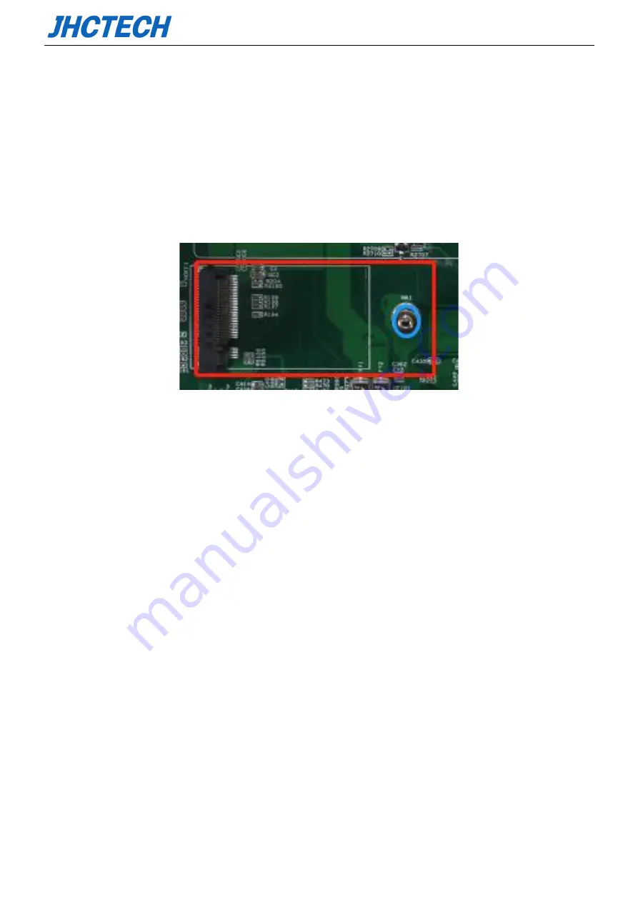
Step 2: Hold the M.2 module with its notch aligned with the NGFF socket of the mother board and insert 

it at a 30 degrees angle into the socket (Note: Pay attention to avoiding the hard disk cable during the 

installation process); 


Step 3: Screw one screw to the holder as shown in the picture. 


Step 4: Follow the reverse steps of disassembly to complete the product installation. 


2.4.5 Installing Expansion Functional Module 

(Note: this operation is only for KMDA-3921/3920, and KMDA-3610 does not support the 

installation of PCIe/PCI expansion module. Here is an example of KMDA-3921, and the installation 

of KMDA-3920 is similar) 

Step 1: The step here is the same as above chapter “2.5.2 Installing Mini PCIe Module -Step 1”, For 

details, please refer to the above chapter “2.5.2 Installing Mini PCIe Module -Step 1” 


Step 2: Unscrew 4 screws on 4 bars, take off 4 bars; 

Summary of Contents for KMDA-3610

Page 1: ...User s Manual KMDA 3921 3920 3610 User s Manual Ver A1 0 Date 25 July 2019 ...

Page 2: ...User s Manual Version Note No Ver Note Date Writer 1 A1 0 first publish 20190725 Tracy Liu ...

Page 3: ...ed to be accurate and reliable However Shenzhen JHC Technology Co Ltd assumes no responsibility for its use nor for any infringements of the rights of third parties which may result from its use Acknowledgements Award is a trademark of Award Software International Inc IBM PC AT PS 2 and VGA are trademarks of International Business Machines Corporation Intel Skylake and Kabylake are trademarks of I...

Page 4: ...ent materials service time and freight Please consult your dealer for more details If you think you have a defective product follow these steps 1 Collect all the information about the problem encountered For example CPU speed JHC products used other hardware and software used etc Note anything abnormal and list any onscreen messages you get when the problem occurs 2 Call your dealer and describe t...

Page 5: ...sident installation This equipment generates uses and can radiate radio frequency energy and if not installed and used in accordance with the instruction manual may cause harmful interference to radio communications However there is no guarantee that interference will not occur in a particular installation If this equipment does cause harmful interference to radio or television reception in which ...

Page 6: ...10 Series Specifications 4 1 6 Mechanical Specifications 5 Hardware Installation 12 2 1 Introduction 13 2 2 Switches setting 13 2 2 1 CLEAR CMOS Clear CMOS Data 13 2 2 2 AT ATX AT ATX Power on mode selection 14 2 3 I O Ports Indication 14 2 3 1 Ethernet Connector LAN 19 2 3 2 USB Connector 19 2 3 3 HDMI 20 2 3 4 DP 21 2 3 5 VGA 21 2 3 6 DIO Connector 22 2 3 7 Power Input Connector DC IN 23 2 3 8 C...

Page 7: ... Sub card ECX 242 29 2 3 20 PCIeX4 Slot In Sub card ECX 241 30 2 3 21 PCIeX16 Slot In Sub card ECX 241 or ECX 242 30 2 3 22 LED 31 2 4 Installation 32 2 4 1 HDD SSD Installation 32 2 4 2 Installing mini PCIe 34 2 4 3 Installing MSATA 39 2 4 4 Installing M 2 Module 39 2 4 5 Installing Expansion Functional Module 40 BIOS Setup 42 3 1 BIOS Description 43 3 1 1 Entering the Setup Utility 43 3 2 BIOS p...

Page 8: ...3 Updating the BIOS 54 Driver Installation 55 4 1 Follow the sequence below to install the drivers 56 4 2 Installation 56 4 3 CPU TEMP LED driver 57 4 4 Utility Software Reference 58 SYSTEM RESOURCE 59 5 1 WDT and GPIO 60 ...

Page 9: ...User s Manual 1 General Information CHAPTER 1 ...

Page 10: ...rds based on their requirements Besides DC 12 24V wide power input It is widely used for Industrial Automation Intelligent Transportation ITS and Machine Vision 1 2 Features Key Features Universal aluminum chassis SGCC frame Intel Skylake S Kabylake S Celeron Core I3 I5 I7 CPU 2 260 pin SODIMM DDR4 2133 2400MHz up to 32GB 1 F mini PCIe with SIM slot support 4G LTE and Wifi BT Expansion KMDA 3921 S...

Page 11: ...enix terminal 16 bit DIO DB25 Female I Port optional 1 LPT USB2 0 DIO or 1 Mini PCIe module interface KMDA 3921 3920 Expansion Interface 1 Full size Mini PCIe PCIeX1 USB with SIM slot PCI PCIe slots KMDA 3921 Series 1 PCIe X16 1 PCIeX1 2 PCI KMDA 3920 Series 1 PCIe X16 1 PCIe X4 KMDA 3610 Series none Storage 1 mSATA 1 M 2 2242 B Key 2 2 5 SATA HDD SSD bay support Raid0 1 In Intel Q170 1 3 2 Displa...

Page 12: ...HDD Airflow Relative humidity 10 90 40 C non condensing Storage temperature 40 85 C 40 185 F Vibration loading during operation With SSD 5 0 Grms random 5 500 Hz With HDD 1 0 Grms random 5 500 Hz Shock during operation With SSD 50g peak acceleration 11 ms duration With HDD 20g peak acceleration 11 ms duration EMC CE FCC Class B 1 5 3921 3920 3610 Series Specifications Model KMDA 3921 KMDA 3920 KMD...

Page 13: ...t Optional LPT 2 USB2 0 16 bit DIO Optional LPT 2 USB2 0 16 bit DIO 16 bit DIO default Expansion 1 mini PCIe 1 M 2 2242 B Key 1 PCIeX16 1 PCIeX1 2 PCI 1 mini PCIe 1 M 2 2242 B Key 1 PCIeX16 1 PCIeX4 Or 2 PCI 1 mini PCIe 1 M 2 2242 B Key 1 6 Mechanical Specifications The KMDA 3921 3920 3610 new industrial design Box computer of JHCTECH consists of a JHC SBC STX I951 a sub card ECD 9050 and an expan...

Page 14: ...User s Manual 6 ECX 242 ECI 245 Note ECX 241 and ECI 245 are 2 alternatives in KMDA 3920 Main Board Front AXM I951 Figure 1 1 Main Board Rear AXM I951 ...

Page 15: ...User s Manual 7 Figure 1 2 Sub card ECD 9050 Figure 1 3 Riser card ECX 241 Figure 1 4 ...

Page 16: ...User s Manual 8 Riser card ECX 242 Figure 1 5 Riser card ECI 245 Figure 1 6 ...

Page 17: ...User s Manual 9 KMDA 3921 Dimension Unit mm Figure 1 7 ...

Page 18: ...User s Manual 10 KMDA 3920 Dimension Unit mm Figure 1 8 ...

Page 19: ...User s Manual 11 KMDA 3610 Dimension Unit mm Figure 1 9 ...

Page 20: ...User s Manual 12 Hardware Installation CHAPTER 2 ...

Page 21: ...er Name Description CLEAR CMOS Clear CMOS Data Setting 3 Pin Switch AT ATX Set Power on mode at AT or ATX 3 Pin Switch 2 2 1 CLEAR CMOS Clear CMOS Data Figure 2 1 If you encounter the followings a CMOS data becomes corrupted b You forget the supervisor or user password you can reconfigure the system with the default values stored in the ROM BIOS To load the default values stored in the ROM BIOS pl...

Page 22: ... on mode selection Figure 2 2 The KMDA 3921 3920 3610 provides a AT ATX SW which users can set Power on mode by it When you dial it at AT it means power on by AC Power When you dial it at ATX it means power on by Power button 2 3 I O Ports Indication KMDA 3921 Front Panel I O Ports Figure 2 3 ...

Page 23: ... 5mm phone jack 1 DP 1 HDMI 1 VGA 1 PS 2 2 USB 2 0 Type A 4 USB3 0 Type A 1 I Port 2 Gigabit LAN RJ45 with LEDs 4 COM DB9 2 RS232 2 RS232 422 485 8 bit DIO 10 pole terminal block 1 PCIeX1 1 PCIeX16 2 PCI slots Power button HDD LED CPU LEDs AT ATX SW Clear CMOS SW KMDA 3921 Rear Panel I O Ports Figure 2 4 The Rear panel I O ports consist of the following 2 SATA SSD HDD ...

Page 24: ...nix terminal block 1 Remote SW 2 pole terminal block 1 Mic 1 Line out 3 5mm phone jack 1 DP 1 HDMI 1 VGA 1 PS 2 2 USB 2 0 Type A 4 USB3 0 Type A 1 I Port 2 Gigabit LAN RJ45 with LEDs 4 COM DB9 2 RS232 2 RS232 422 485 8 bit DIO 10 pole terminal block 1 PCIeX4 1 PCIeX16 slots or 2 PCI slots Power button HDD LED CPU LEDs AT ATX SW Clear CMOS SW ...

Page 25: ...User s Manual 17 KMDA 3920 Rear Panel I O Ports Figure 2 6 The Rear panel I O ports consist of the following 2 SATA SSD HDD KMDA 3610 Front Panel I O Ports Figure 2 7 ...

Page 26: ...ine out 3 5mm phone jack 1 DP 1 HDMI 1 VGA 1 PS 2 2 USB 2 0 Type A 4 USB3 0 Type A 2 Gigabit LAN RJ45 with LEDs 4 COM DB9 2 RS232 2 RS232 422 485 8 bit DIO 10 pole terminal block 16 bit DIO DB25 Female Power button HDD LED CPU LEDs AT ATX SW Clear CMOS SW KMDA 3610 Rear Panel I O Ports Figure 2 8 The Rear panel I O ports consist of the following 2 SATA SSD HDD ...

Page 27: ...nal Pin 10 100 1000BaseT Signal 1 TX 10 100 LAN_DA GHz 5 LAN_DC GHz 2 TX 10 100 LAN_DA GHz 6 RX 10 100 LAN_DB GHz 3 RX 10 100 LAN_DB GHz 7 LAN_DD GHz 4 LAN_DC GHz 8 LAN_DD GHz 2 3 2 USB Connector The USB device allows data exchange between your computer and a wide range of simultaneously accessible external Plug and Play peripherals The KMDA 3921 3920 3610 provides 4 USB3 0 3 USB2 0 one inside for...

Page 28: ...D 9 StdA_SSTX 5 StdA_SSRX Shell Shield 2 3 3 HDMI The KMDA 3921 3920 3610 provides a high resolution HDMI display port They can support the most resolution up to 3840 2160 30Hz Table 2 4 for HDMI pin assignments Figure 2 12 Table 2 4 HDMI Pin Assignments Pin Signal Pin Signal Pin Signal 1 DATA2_P 8 GND 15 SCL 2 GND 9 DATA0_N 16 SDA 3 DATA2_N 10 CLK_P 17 GND 4 DATA1_P 11 GND 18 VCC ...

Page 29: ...ents Figure 2 13 Table 2 5 DP Pin Assignments Pin Signal Pin Signal Pin Signal 1 DATA0_P 8 GND 15 AUXP 2 GND 9 DATA2_N 16 GND 3 DATA0_N 10 DATA3_P 17 AUXN 4 DATA1_P 11 GND 18 HPD 5 GND 12 DATA3_N 19 GND 6 DATA1_N 13 CTRL 20 PWR 7 DATA2_P 14 GND 2 3 5 VGA The KMDA 3921 3920 3610 provides a VGA ports via a D sub 15 pin connector it supports the most resolution up to 1920 1200 60Hz Table 2 6 for DP p...

Page 30: ...Pin 8 bit DIO terminal connector in rear Table 2 7 for Pin assignments Figure 2 15 Table 2 7 8 bit DIO Pin Assignments Pine DIO Signal Pin DIO Signal 1 GP70 2 GP71 3 GP72 4 GP73 5 GND 6 GP74 7 GP75 8 GP76 9 GP77 10 5V The KMDA 3610 provides 8 bit 16 bit DIO The 8 bit DIO definition is identical to the above mentioned KMDA 3921 3920 8 bit DIO definition The other 16 bit DIO is derived from a DB25 f...

Page 31: ... NC 7 GPIO7 16 GPIO11 25 NC 8 GPIO8 17 GPIO12 9 5V 18 GPIO13 All of the above DIOs are TTL signals digital inputs high level 1 2 5 25V low level 0 0 0 8V digital output high level 1 minimum 2 4V low level 0 Maximum 0 4V 2 3 7 Power Input Connector DC IN The KMDA 3921 3920 3610 provides a wide power input DC 12 24V by a 3 pin terminal Table 2 9 for pin assignments Figure 2 17 Table 2 9 DC IN port p...

Page 32: ...r pin assignments Figure 2 18 Table 2 10 COM1 2 Serial Ports Pin Assignments Pin RS 232 Signal RS 422 Signal RS 485 Signal 1 DCD TX DATA 2 RxD TX DATA 3 TxD RX NC 4 DTR RX NC 5 GND GND GND 6 DSR NC NC 7 RTS NC NC 8 CTS NC NC 9 RI NC NC 2 3 9 COM3 4 Connector Figure 2 19 COM3 4 are only for RS232 The Pin assignments are as follows Table 2 11 COM3 4 Serial Port Pin Assignments Pin Signal Pin Signal ...

Page 33: ...Figure 2 20 Table 2 12 PS 2 Pin Assignments Pin Signal Pin Signal 1 SIO_KDAT 4 VCC 2 SIO_MDAT 5 SIO_KCLK 3 GND 6 SIO_MCLK 2 3 11 Remote Switch signal Connector For the remote switch signal interface of the switch machine the terminal of the motherboard coastline is a 2 pin terminal Table 2 13 for pin assignments Figure 2 21 Table 2 13 Remote Switch Pin Assignments Pin Signal 1 PWR_BTN 2 GND ...

Page 34: ...User s Manual 26 2 3 12 Serial ATA1 S_SATA1 S_SATA2 Figure 2 22 Table 2 14 for pin assignments Table 2 14 Serial ATA1 pin assignments Pin Signal Pin Signal 1 GND 5 RX 2 TX 6 RX 3 TX 7 GND 4 GND ...

Page 35: ...R2 Figure 2 23 Table 2 15 for pin assignments Table 2 15 SATA power connector Pin Signal Pin Signal 1 5V 3 GND 2 GND 4 12V 2 3 14 mSATA Connector MSATA1 Figure 2 24 MSATA interface with SATA and USB signal The Serial ATA connectors are used to connect mSATA module ...

Page 36: ... slot Note SIM1 slot is connected to 3GWIFI1 slot 2 3 16 SIM card connector SIM1 SIM1 slot is connected to 3GWIFI1 slot 2 3 17 M 2 connector NGFF1 M 2 NGFF interface with USB2 0 and SATA signal Install M 2 2242 B Key modules such as SATA SSD module that comply to the M 2 2242 B Key specifications into the NGFF slot 2 3 18 PCI Slot In Sub card ECX 242 or ECI 245 The KMDA 3921 provides two PCI expan...

Page 37: ...ion control cards and data acquisition cards The length of the expansion card should be less than 235mm 2 3 19 PCIeX1 Slot In Sub card ECX 242 The KMDA 3921 provides PCIeX1 expansion slot from the ECX 242 daughter card used for connecting standard PCIeX1 device The length of the expansion card should be less than 225mm ...

Page 38: ...ice The length of the expansion card should be less than 225mm 2 3 21 PCIeX16 Slot In Sub card ECX 241 or ECX 242 The KMDA 3921 provides PCIeX16 expansion slot from the ECX 242 daughter card The KMDA 3920 provides PCIeX16 expansion slot from the ECI 241 used for connecting standard PCIeX16 devices such GPU cards The length of the expansion card should be less than 225mm ...

Page 39: ...1 HDD LED 3 CPU temperature class LEDS on the front Users can monitor the working state of the CPU according to the display of LEDs Table 2 30 for LEDs state of CPU temperature class Table 2 30 LEDs state of CPU temperature class LED State Red Warning Yellow High Green Normal ...

Page 40: ...n Step 1 Unscrew 4 screws on the HDD SSD cover remove the HDD SSD cover Step 2 Unscrew 2 screws on HDD SSD bay take out the HDD SSD bay Step 3 Put the HDD SSD into the HDD SSD bay screw 4 screws as the picture shows Step 4 Put the HDD SSD bay into the HDD SSD slot as the picture shows Step 5 Screw 2 screws on the HDD SSD bay Step 6 Install the HDD SSD cover screw 4 screws as the picture shows ...

Page 41: ...User s Manual 33 ...

Page 42: ...A 3921 3920 Unscrew screws on the Mounting brackets as picture shows remove the mounting bracket Note There are three types of mounting brackets please disassemble according to your actual situation Unscrew the Spring screw and take off the expansion cover ...

Page 43: ...User s Manual 35 Installation mode I of KMDA 3921 3920 Installation mode II of KMDA 3921 3920 ...

Page 44: ...User s Manual 36 Installation mode III of KMDA 3921 3920 ...

Page 45: ...User s Manual 37 KMDA 3610 Unscrew the 7 screws on the bottom cover 4 in front back 3 in side as shown in the picture remove the bottom cover ...

Page 46: ...e module with its notch aligned with the Mini PCIe socket of the board and insert it at a 30 degrees angle into the socket Step 3 Screw one screw to the holder Step 4 Follow the reverse steps of disassembly to complete the product installation ...

Page 47: ...notch aligned with the MSATA socket of the mother board and insert it at a 30 degrees angle into the socket Note Pay attention to avoiding the hard disk cable during the installation process Step 3 Screw one screw to the holder as shown in the picture Step 4 Follow the reverse steps of disassembly to complete the product installation 2 4 4 Installing M 2 Module Step 1 The step here is the same as ...

Page 48: ... in the picture Step 4 Follow the reverse steps of disassembly to complete the product installation 2 4 5 Installing Expansion Functional Module Note this operation is only for KMDA 3921 3920 and KMDA 3610 does not support the installation of PCIe PCI expansion module Here is an example of KMDA 3921 and the installation of KMDA 3920 is similar Step 1 The step here is the same as above chapter 2 5 ...

Page 49: ...User s Manual 41 Step 3 Put the PCIe PCI functional module into the expansion slot which is on the ECX 242 Step 4 Follow the reverse steps of disassembly to complete the product installation ...

Page 50: ...User s Manual 42 BIOS Setup CHAPTER 3 ...

Page 51: ...gs as follows 1 An error message appears on the screen during the system self test and asks for the SETUP setting 2 You want to change the factory default settings based on customer characteristics But in general customers are not recommended to set it up In most cases using the default value is already the best setting The BIOS Setup Utility enables you to configure Hard drives diskette drives an...

Page 52: ...g boxes that prompt you to verify that you wish to execute that option Other options lead to dialog boxes that prompt you for information Some options marked with a triangle lead to submenus that enable you to change the values for the option Use the cursor arrow keys to scroll through the items in the submenu In this manual default values are enclosed in parenthesis Submenu items are denoted by a...

Page 53: ...al Help F2 Previous Values F3 Optimized Defaults F4 Save Exit 3 2 2 Main Menu When you enter the BIOS Setup program the main menu appears giving you an overview of the basic system information Select an item and press Enter to display the submenu Press Esc to back to the main menu The BIOS setup program provides a help screen You can call up this help screen from any menu by simply pressing the F1...

Page 54: ...tion This item shows the basic information about the currently used processor including name type speed ID core Microcode version etc IGFX VBIOS Version This item shows the Current VBIOS version of the CPU integrated graphics Total Memory This item shows the total memory size of the current motherboard Memory Frequency This item shows the current memory operating frequency PCH Information This ite...

Page 55: ...Set the language interface of the BIOS System Date Set the date The format of the date is week month day year System Time Set the time The format of the time is hour minute second 3 2 3 Advanced Menu This page sets up more advanced information about your system Handle this page with caution Any changes can affect the operation of your computer CPU Configuration ...

Page 56: ...this sub menu there will be the setting of the encryption security module the motherboard will install the encryption module hardware will take effect ACPI Settings Advanced configuration and power management interface settings enter this submenu there will be ACPI related settings COM setting COM port settings enter this sub menu there will be set COM working mode RS422 RS232 RS485 Hardware Monit...

Page 57: ...ub menu there will be various settings to support UEFI startup and non UEFI startup If you need to start the traditional MBR device you need to enable CSM Turning off the CSM turns it into a pure UEFI boot USB Configuration USB configuration enter this sub menu there will be USB related detailed settings 3 2 4 Chipset Menu The chipset menu items allow you to change the settings for the North Bridg...

Page 58: ...graphics related settings PEG Port Configuration PEG graphics configuration enter this sub menu there will be related settings for the external graphics card PCH IO Configuration South Bridge Configuration SATAAnd RST Configuration SATA hard disk and fast storage configuration enter this sub menu there will be related settings of the hard disk HD Audio Configuration High fidelity audio which contr...

Page 59: ...User s Manual 51 3 2 5 Security menu Administrator Password This item sets the information of the administrator password User Password This item sets the information of the normal user password ...

Page 60: ...the quick start function on or off When set to Enabled the system will skip some detection items and reduce the startup time Set Boot Priority Start device priority settings If the user wants to install the operating system please set Boot Option 1 as your CD ROM device or your U disk device make sure that your CD ROM drive has an operating system or your U disk has a PE system After the setting i...

Page 61: ... to save the changes that you have made and reset Discard Changes and Reset This item enables you to discard the changes that you have made and reset Save Changes This item enables you to save the changes that you have made Discard Changes This item enables you to discard the changes that you have made Restore Defaults This item enables you to restore the system defaults Save as User Defaults This...

Page 62: ...e bridge between hardware and operating system Now hardware and various applications are constantly updated When your system encounters problems such as the system does not support the latest published CPU you need to upgrade your BIOS NOTE 1 Only upgrade the BIOS if you encounter problems and need to 2 To upgrade the BIOS please use the BIOS read write program attached to our driver CD or downloa...

Page 63: ...User s Manual 55 Driver Installation CHAPTER 4 ...

Page 64: ...llations 4 2 Installation Insert the AXM I951 CD ROM into the CD ROM drive And install the drivers in turn Step 1 Install AMT Driver 1 Double click on the AMT folder and double click on the Setup exe 2 Follow the instructions that the window shows 3 The system will help you install the driver automatically Step 2 Install Audio Driver 1 Double click on the Audio folder and double click on the Setup...

Page 65: ...atically Step 7 Install USB3 0 Driver 1 Double click on the USB3 0 folder and double click on the Setup exe 2 Follow the instructions that the window shows 3 The system will help you install the driver automatically Step 8 Install VGA Driver 1 Double click on the VGA folder and double click on the Setup exe 2 Follow the instructions that the window shows 3 The system will help you install the driv...

Page 66: ...iant They are provided only for the convenience of the customer The following software is furnished under license and may only be used or copied in accordance with the terms of the license These software s are subject to change at any time without prior notice Please refer to the support disk for available software ...

Page 67: ...User s Manual 59 SYSTEM RESOURCE CHAPTER 5 ...

Page 68: ...r with jhctech_init release the library s occupied resources when not needed 3 parameter description 4 creation date 5 1 void watchdog_set int time 2 function description Watchdog function 3 parameter description time is to Set the dog feeding time Value between 0 and 255 Setting 0 means to turn off the watchdog 4 creation date 5 1 void smbus_16pin_gpio_mode int port int mode 2 function descriptio...

Page 69: ... int port int level 2 function description high and low levels output of the subcard 3 parameter description Parameter port represents the number of the GPIO 1 or 2 Level 8 bit of a bit each bit controls a GPIO pin output value Bit 1 means output high level Bit 0 means output low level Note The output value is valid only when the pin is in output mode 4 creation date 5 Return value Bit7 Bit6 Bit5 ...

Page 70: ...level state of a GPIO pin parameter port fill in sub card GPIO number 1 or 2 Note The read value is valid only when the pin is in input mode 4 creation date 5 Note If you want more programs of the motherboard s watchdog and subcard s GPIO please call 86 0755 86021176 8021 86 0755 86021176 8023 for more information Return value Bit7 Bit6 Bit5 Bit4 Bit3 Bit2 Bit1 Bit0 GPIO pin PIN8 PIN7 PIN6 PIN5 PI...

Reviews: