User’s Guide
10
2.1 Introduction
The following sections show the internal switch settings and the external connectors and pin assignments
for applications.
2.2 Switches
The KMDA-3230 Box Computer has a number of switches on the panel that allows you to configure your
system to suit your application. The table below shows the function of each of the board’s switches:
Switches
Name
Description
SW1
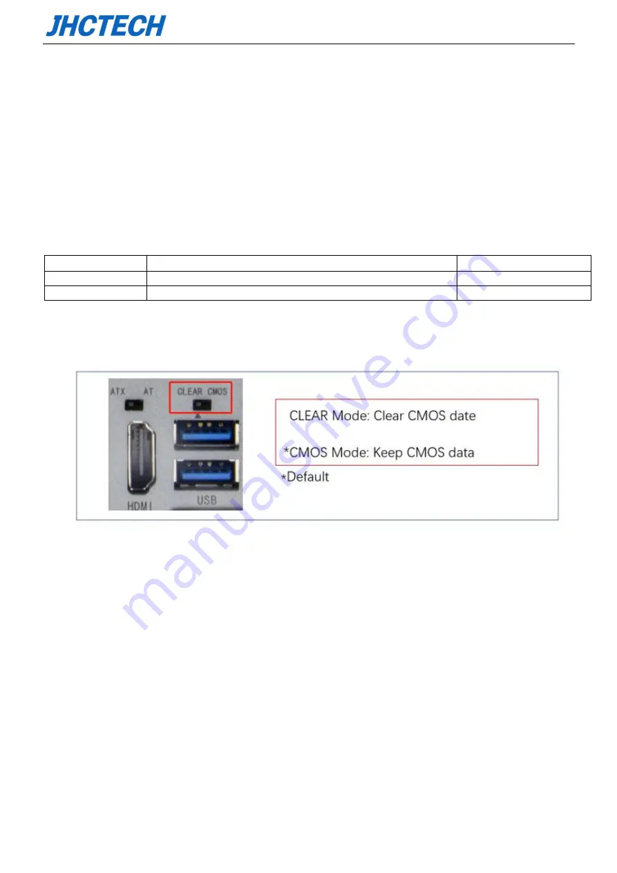
Clear CMOS Data Setting
3-Pin Switch
SW2
Set Power-on mode at AT or ATX
3-Pin Switch
2.2.1 SW1-Clear CMOS Data
Figure 2. 1
If you encounter the followings
a) CMOS data becomes corrupted.
b) You forget the supervisor or user password.
You can reconfigure the system with the default values stored in the ROM BIOS.
To load the default values stored in the ROM BIOS, please follow the steps below.
1. Power-off the system and unplug the power cord.
2. Dial the dip switch to CLEAR mode, stay for 5~6 seconds, and then revert to CMOS mode;
3. Power-On the computer, press the Del key to enter the BIOS setting and reload the optimal default
value;
4. Save and exit the Settings.
Summary of Contents for KMDA-3230
Page 1: ...User s Guide User s Guide KMDA 3230 Ver A1 0 Date 01 Jul 2020 ...
Page 2: ...User s Guide Version Note No Ver Note Date Writer 1 A1 Final publish 20200701 Echo Guo ...
Page 10: ...User s Guide 1 General Information CHAPTER 1 ...
Page 16: ...User s Guide 7 Figure 1 4 KMDA 3230 Rear Panel Figure 1 5 ...
Page 17: ...User s Guide 8 KMDA 3230 Dimension Unit mm Figure 1 6 ...
Page 18: ...User s Guide 9 Hardware Installation CHAPTER 2 ...
Page 36: ...User s Guide 27 ...
Page 43: ...User s Guide 34 BIOS Setup CHAPTER 3 ...
Page 51: ...User s Guide 42 ...
Page 60: ...User s Guide 51 External Gfx Card Primary Display Configuration ...
Page 63: ...User s Guide 54 USB Configuration ...
Page 69: ...User s Guide 60 Driver Installation CHAPTER 4 ...


