69-0058Rev. D
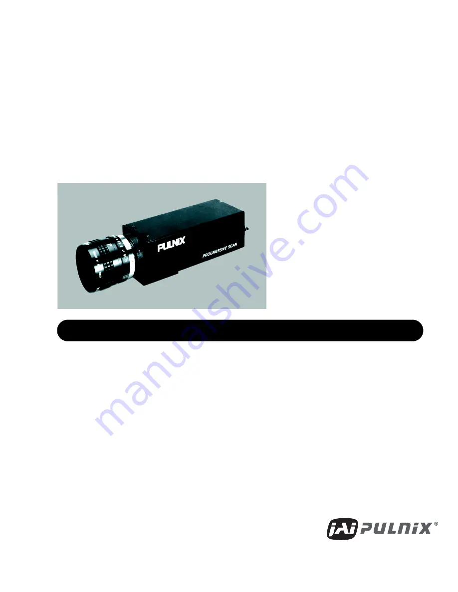
TM-6710/6710CL High-Speed Progressive Scanning CCD Camera
I m a g i n g P r o d u c t s
O p e r a t i o n M a n u a l
Page 1: ...69 0058 Rev D TM 6710 6710CL High Speed Progressive Scanning CCD Camera I m a g i n g P r o d u c t s O p e r a t i o n M a n u a l ...
Page 2: ......
Page 3: ...note that the use of interconnect cables that are not properly grounded and shielded may affect CE compliance Contact PULNiX Applications Engineering Department for further information regarding CE compliance FCC This equipment has been tested and found to comply with the limits for a Class A digital device pursuant to Part 15 of the FCC Rules These limits are designed to provide reasonable protec...
Page 4: ......
Page 5: ...k focusing the Lens 11 3 Operation 12 3 1 Dual Tap Video Output 12 3 2 Rear Panel 12 3 2 1 Mode Control Switches TM 6710 14 3 3 Modes of Operation 14 3 3 1 Shutter Operation 14 3 3 2 External Synchronization 15 3 3 3 Asynchronous Reset with Shutter 15 3 3 4 Partial Scan Mode 18 3 3 5 Integration 18 3 3 6 Progressive scanning 19 3 3 7 RS 232C or optional RS 485 Control and Camera Link Serial Commun...
Page 6: ...ommunication Cable 10 FIGURE 8 Rear Panel Layout TM 6710 12 FIGURE 9 Rear Panel Layout TM 6710CL 13 FIGURE 10 External Pulse Width Mode 16 FIGURE 11 Internal Fast Reset Mode 17 FIGURE 12 Internal Slow Reset Mode 18 FIGURE 13 Async Reset Image Capture 25 FIGURE 14 Integrated Image Capture 25 FIGURE 15 TM 6710 Physical Dimensions 34 FIGURE 16 TM 6710CL Physical Dimensions 34 FIGURE 17 Glass Specific...
Page 7: ...onic shutter The substrate drain electronic shutter captures images at various speeds without any smearing The electronic shutter works in all there scanning modes except slow speed at partial scanning 1 2 progressive scan interline transfer CCD Advantages include High resolution 648 H x 484 V active pixels for very high speed and image quality Square pixels 9 0 x 9 0 µm Precise dimensional measur...
Page 8: ...amera Link The Camera Link model is called the TM 6710CL RS 232C or RS 485 control External computer control allows the operator to remotely adjust the following functions clock speed shutter gain A D reference and scan format Camera Link controls the same functions via a Camera Link serial communication VGA display output Because progressive scan cameras are not in TV format the display of the vi...
Page 9: ...CL System Configuration Figure 2 below presents a typical system configuration for the TM 6710CL camera Please see Power Supply and Power Cable Setup on page 7 for information on power supplies VIDEO POWER SHUTTER 0 1 2 3 4 5 6 7 8 9 DWN UP MODE DIGITAL 1 0 2 3 4 5 6 7 8 9 A B C D E Frame Grabber Board Multi Sync Analog Monitor Ext Sync Power Trigger Analog video RS 232 P N CS 232 B912 Digital cab...
Page 10: ...t the Components List below to assure that you have received everything as ordered and that nothing has been overlooked in the packing materials If any item is missing please contact your PULNiX representative immediately TM 6710 or TM 6710CL camera Tripod mount TM 6710 TM 6710CL manual if ordered Warranty card Document information card 2 1 3 Accessories and Options Following is a list of addition...
Page 11: ...le is shown below For the TM 6710CL serial communication camera control is done via the Camera Link connector on the rear panel of the camera Pin Description Pin Description 1 GND Power 7 VD In 2 12V DC 8 N C 3 GND Analog 9 HD In 4 Video Out 10 RXD RS 232 5 GND Digital 11 Integration 6 VINIT In 12 TXD RS 232 Pin Description Pin Description 1 GND Power 7 VD In 2 12V DC 8 N C 3 GND Analog 9 HD In 4 ...
Page 12: ...The connector pinout is shown in Figure 4 below FIGURE 4 Camera Link Connector Pin Description Pin Description Pin Description 1 A0 18 CLK 35 CLK 2 B0 19 A0 36 GND 3 A1 20 B0 37 VCC jumper 4 B1 21 A1 38 VCC jumper 5 A2 22 B1 39 EXT HD 6 B2 23 A2 40 TXD 7 A3 24 B2 41 LPULSE 8 B3 25 A3 42 RXD 9 A4 26 B3 43 VINIT 10 B4 27 A4 44 INTEG 11 A5 28 B4 45 EXP 12 B5 29 A5 46 EXP 13 A6 30 B5 47 LDV 14 B6 31 A...
Page 13: ... to prevent exposed leads from touching The 12V lead is marked with a red stripe or white lettering be sure not to reverse the leads All connections must be properly insulated to prevent shorting If using PULNiX power cables such as the 12P 02S etc please refer to the pin out diagram The color coded leads use Gray for Ground and Yellow for 12V DC FIGURE 6 12P 02S Power Cable Note Make sure that th...
Page 14: ...onnector while applying slight pressure until the keyways line up Press the connector into place until it is firmly seated You may now plug the power cord into the 110V AC socket and power up the camera 2 2 3 RS 232 Cables and Connectors TM 6710 only FIGURE 7 RS 232 Serial Communication Cable 12 Pin Male Connector 12 Pin Female Connector Pin Description Pin Description 1 GND 1 GND 2 12V 2 12V 3 GN...
Page 15: ...ount lens to the camera carefully engage the threads and rotate the lens clockwise until it firmly seats on the mounting ring Do not force the lens if it does not seat properly Please note that some lenses with extremely long flangebacks may exceed the mounting depth of the camera 2 2 6 Back Focusing the Lens To backfocus the TM 6710 camera follow the steps below 1 Attach a C mount lens in the len...
Page 16: ...twice per horizontal blanking period Lines are grouped in twos so that 1 and 2 and 3 and 4 and so on are output from channel A and B simultaneously 3 2 Rear Panel FIGURE 8 Rear Panel Layout TM 6710 1 2 3 4 5 Channel A Channel B V shift registers Photodiode CCD output Horizontal shift registers Lines Odd Even VIDEO POWER SHUTTER 0 1 2 3 4 5 7 8 9 DWN UP MODE DIGITAL 1 0 2 3 4 5 6 7 8 9 A B C D E 6 ...
Page 17: ...Page 11 Operation TM 6710 6710CL High Speed Progressive Scanning CCD Camera FIGURE 9 Rear Panel Layout TM 6710CL POWER CAMERA LINK 12 Pin Power Camera Link connector ...
Page 18: ...A B fine tune up increase gain of Ch A down decrease gain of Ch A while decrease increase gain of Ch B at 5 1 ration 3 Main Vref control up increase gain of Ch A down decrease A D voltage reference of Ch A Ch B 4 Vref balance control up increase gain of Ch A down increase decrease A D voltage reference of Ch A while decrease increase gain of Ch B 5 Gain selection up 9dB down 12dB 6 Gain selection ...
Page 19: ...lect from 1 to 9 the TM 6710 s asynchronous camera discharges the photo charges into the substrate drain although the camera is still running on its sync timing and only outputs captured video When the negative going reset pulse is applied the camera will latch the falling edge to its next horizontal drive and reset vertical sync timing immediately Then it starts integrating for the period of shut...
Page 20: ... internal VINIT will be generated at the following edge positive going edge of the external pulse resetting the internal timing including the video sync The shutter speed is the same as the external pulse width but the integration delays 5H from the leading edge For the immediate reset option please contact PULNiX FIGURE 10 External Pulse Width Mode For the progressive format one frame of video ou...
Page 21: ...delay The shutter speed is controlled by the dial switch FIGURE 11 Internal Fast Reset Mode 3 3 3 c Internal Slow Reset Mode The speed control ranges from 1 120 to 1 4 000 sec With the internal slow reset mode selected the camera operates the reset and shutter in the same way as the external pulse width control mode When the external VINIT pulse is applied internal VINIT is latched to HD and the s...
Page 22: ...for the TM 6710CL LVDS During low the TM 6710 series keeps integrating and upon the rising edge of the INTEG control pulse outputs the frame During integration the signal processing keeps optical black levels as the reference black video to clamp video levels This has the result of cancelling out thermal noise during the integration period 7H Hd Internal Vinit Transfer Gate Pulse Discharge pulse C...
Page 23: ...video processing into 75ohms 1Vp p output format 2 Partial scanning output Rear switch 100 lines 200 lines TM 6710 only By setting the switch to 100 line partial scan the TM 6710 outputs 100 lines of video It repeats the same rate with the fast dump blanking The asynchronous reset and electronic shutter functions are maintained at each partial scan When 200 line partial scan is selected 200 lines ...
Page 24: ... When the process is completed it sends a completion signal AK packet If an error is detected a No go signal NK packet is sent back and it disregards the packet signal in the buffer When an NK packet is sent from the TM 6710 the host must correct the error and resend the packet Example Executing manual shutter control 2 The C C packet is sent as follows S M 2 CR 3AH 53H 4DH 32H 0DH where S Shutter...
Page 25: ... the A channel and the B channel The GA and GB commands fine tune the gain of the A and B channels respectively to achieve balance The ratio is about 5 1 Examples GM D2 CR D2 gain 210 3AH 47H 46H 46H 0DH GA 12 CR 3AH 47H 31H 32H 0DH Gain control value 18 Command V Function A D reference voltage control In the default gain setting there is no shutter The A D reference voltage bottom is preset to 0 ...
Page 26: ...57H 41H 36H 0DH Page 0 is factory use only Saving the current gain setting to User Table A with the WU command W U A CR 3AH 57H 55H 41H 0DH Command L Function Select and read a memory page and set the preprogrammed data This loads the data from the preset page location or preset gain table L P 6 CR 3AH 4CH 50H 36H 0DH Command R Function Output data values of camera memory PULNiX software is availa...
Page 27: ...R 3AH 43H 30H 0DH Note When RS 232C is active back plate switches are overwritten and do not function In order to activate back plate switches power off and power up again 1 Main Gain ch A and ch B 2 Ch A fine tune gain 3 Ch B fine tune gain 4 Ch A video voltage reference 5 Ch B video voltage reference 6 Reserved 7 Video voltage reference top 8 Reserved 9 Function flag 10 Shutter dial switch valve...
Page 28: ...top voltage setting Vbottom Vsub setting W Write P Page U User S System 0 6 A D A D ACK ACK ACK Write to P EPROM Write to U EPROM Write to S EPROM L Load P Page U User S System 0 6 A D A D ACK ACK ACK Load from P EPROM Load from U EPROM Load from S EPROM R Report R Current P Page U User S System X Execute D Date 0 6 A D A D ACK ACK ACK ACK ACK DATE ACK RR 12x2 bytes ACK P 9 F 12x2 bytes ACK U 9 F ...
Page 29: ...l signal with EIA 644 format 100ohms output termination impedance Output from 51 pin connector Mating connector Airborne MQ3130511130000 Please consult digital cable information e g 50DG 02LP 2m cable The TM 6710CL uses the 26CL 02 26 Camera Link cable 3 3 9 b Line Data Valid Differential line driven signal with EIA 644 format It is active high side is higher than side during the transfer of each ...
Page 30: ...line driven signal with EIA 644 format It is active high during the transfer of each frame data During integration both LDV and FDV are kept high and restart upon the completion of integration 3 3 9 d Pixel Clock Differential line driven signal with EIA 644 format The master clock frequency is 50 98MHz or 40 068MHz ...
Page 31: ...d Clock to Data Ready Tdc Data Ready to Next Clock Thd Data Hold Time Pixel Clock Data A B Tcd 6 7_nsec Tdc 71 7_nsec Thd 2 3_ nsec 2 Horizontal Signals External HD Internal HD LDV Digital Data Analog Video fHD 15 24 KHz tHD 65 6 msec A 8p 0 619msec C 836 P 65 6msec B 759 P 59 6msec F 836 P 65 6msec E 694 P 54 4msec D 142 P 11 2msec G 1 P 0 08msec H 148 P 11 61msec I 648 P 50 8msec J 168 P 6 59mse...
Page 32: ... 16 66 msec B 0 H 12 µsec C 4 5 H 295 µsec D 249 5 H 16 37 ms E 254 H 16 66 ms F 3 H 196 7 µsec I 2 H 131 2 µsec L 3 H 98 39 µsec P 6 H 196 79 µsec G 5 H 0 328 ms J 7 H 0 459 ms M 18 H 0 59 ms N 3 H 98 39 µsec H 249 H 16 33 ms K 242 H 15 87 ms O 484 H 15 87 ms S 249 5 H 16 37 ms T 254 H 16 66ms Y 237 H 15 55 ms CC 484 H 15 94 ms Q 1 H 65 59 µsec U 3 H 196 79 µsec AA 18 H 0 59 ms X 7 H 0 459 ms BB ...
Page 33: ...dy Tdc Data Ready to Next Clock Thd Data Hold Time Pixel Clock Data A B Tcd 6 9_nsec Tdc 32 3_nsec Thd 2 6_ nsec 2 Horizontal Signals External HD Internal HD LDV Digital Data Analog Video fHD 30 49 KHz tHD 32 8 µsec A 16P 0 619 µsec C 836 P 32 8 µsec B 760 P 29 8 µsec F 836P 32 8 µsec E 694 P 27 23 µsec D 142 P 5 57 µsec G 1 P 0 04 µsec H 150 P 5 85 µsec I 648 P 25 42 µsec J 168 P 3 3 µsec K 648 P...
Page 34: ... 254 H 8 33 msec B 0 H 6 µsec C 4 5 H 147 6 µsec D 249 5 H 8 18 ms E 254 H 8 33 ms F 3 H 98 4 µsec I 2 H 65 6 µsec L 3 H 49 2 µsec P 6 H 98 4 µsec G 5 H 0 164 ms J 7 H 0 23 ms M 18 H 0 295 ms N 3 H 49 2 µsec H 249 H 8 17 ms K 242 H 7 94 ms 0 484 H 7 94 ms S 249 5 H 8 18 ms T 254 H 8 33 ms Y 237 H 7 77 ms CC 484 H 7 94 ms Q 1 H 32 8 µsec U 3 H 98 4 µsec AA 18 H 0 295 ms X 7 H 0 23 ms BB 3 H 49 2 µs...
Page 35: ...lies Power cables Main power source Shutter control Async mode Lens Proper level setting as Camera Link CC1 and CC2 5 1 2 Symptom Dark Video Remedies Check that the following are properly connected and operational Shutter selection Iris opening on the lens Proper power DC level 5 1 3 Symptom Non Synchronized Video Remedies Check that the following are properly connected and operational Proper mode...
Page 36: ...on and Support Resources For further information and support Phone 408 747 0300 800 445 5444 800 3 PULNIX 24 hour message access Fax 408 747 0660 E mail imaging jaipulnix com Mail JAI PULNiX Inc Sales Department 1330 Orleans Drive Sunnyvale CA 94089 ATTN Video Applications Web Site www pulnix com ...
Page 37: ...68 MHz 20 034 MHz optional TV resolution 500 H x 484 V Min illumination 4 lux at normal speed 120 frame sec S N ratio 45 dB min AGC off Video output 8 bit digital output via RS 644 8 bit x 2 dual or single channel Output clock 25 49 MHz for dual channel output Analog 1 0 Vp p composite video 75ohms sync negative non interlace Display mode video Analog only fHD 30 49 KHz fVD 60 Hz 60 Hz mode AGC OF...
Page 38: ...imensions 39 6 mm 141 2 mm 1 4 20 UNC 2B 2x M6x1 PROGRESSIVE SCAN 7 0 mm 31 7 mm 2X 11 0mm 128 0 mm 46 1 mm 30 0 mm 2x M3x8 VIDEO POWER SHUTTER 0 1 2 3 4 5 7 8 9 DWN UP MODE DIGITAL 1 0 2 3 4 5 6 7 8 9 A B C D E 6 39 6 mm 136 6 mm 1 4 20 UNC 2B 2x M6x1 PROGRESSIVE SCAN 7 0 mm 31 7 mm 2X 11 0mm 128 2 mm 46 3 mm 30 0 mm 2x M3x8 POWER CAMERA LINK ...
Page 39: ...amera FIGURE 17 Glass Specifications FIGURE 18 TM 6710 Spectral Response CCD CCD glass BD 64 Cover glass BK 7 Wave Length nm SPECTRAL RESPONSE 300 400 500 600 700 800 900 1000 0 0 2 0 1 0 3 0 4 0 5 0 6 0 7 0 8 0 9 1 0 Relative Sensitivity 1100 Peak quantum efficiency 38 ...
Page 40: ...GURE 19 TM 6710 Block Diagram FIGURE 20 TM 6710CL Block Diagram CCD CDS A D MPU CDS A D FIF0 Sync Gen FIF0 Control LUT EPROM RS 644 Ch A RS 644 Ch B Timing Gen D A Sync PLL Clock RS 232 FIF0 CCD CDS A D MPU CDS A D FIF0 Sync Gen FIF0 Control LUT EPROM Timing Gen D A Sync PLL Clock FIF0 Camera Link ...
Page 41: ......
Page 42: ...I PULNiX Inc 1330 Orleans Drive Sunnyvale CA 94089 Tel 408 747 0300 Tel 800 445 5444 Fax 408 747 0660 w w w j a i p u l n i x c o m I m a g i n g P r o d u c t s 69 0058 Rev D Email imaging jaipulnix com ...