REL0.1
Page 61 of 95
Kintex Ult FPGA SOM Hardware User Guide
iWave Systems Technologies Pvt. Ltd.
2.8.3
Power & Reset Input
The Kintex Ult FPGA SOM works with 5V power input (VCC) from Board-to-Board Connector2 and generates all other
required powers internally On-SOM itself. SOM power can be enabled/disabled from the carrier board through SOM Power enable
pin (pin232) in Board-to-Board Connector1. Also, in Board-to-Board Connector2, Ground pins are distributed throughout the
connector for better performance.
The Kintex Ult FPGA SOM supports VRTC_3V0 coin cell power input from Board-to-Board Connector2 and connected to
PMIC’s
VBBAT pin for real time clock backup voltage.
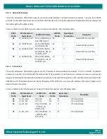
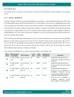
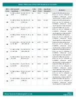
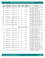
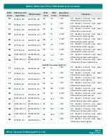
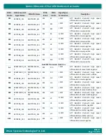
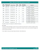
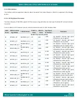
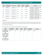
For more details on Power pins on Board-to-Board Connector2, refer the below table.
B2B-2
Pin No
B2B Connector2
Signal Name
FPGA Pin
Name
FPGA
Bank
FPGA Pin
No
Signal Type/
Termination
Description
1, 2, 3, 4, 5, 6, 7, 8, 9,
10, 11, 12, 13,14, 15,
16, 17, 18, 19, 20
VCC_5V
NA
NA
NA
I, 5V Power
Supply Voltage.
21, 23, 37, 43, 49, 55,
73, 107, 113, 119, 129,
167, 173, 179, 185,
191, 197, 203, 209,
215, 221, 227, 233,
239, 22, 24, 30, 74,
108, 114, 120, 130,
168, 174, 180, 186,
192, 198, 204, 210,
216, 222, 228, 234,
240
GND
NA
NA
NA
Power
Ground.
68
VRTC_3V0
NA
NA
NA
I, 3V Power
3V backup coin cell input for
RTC.

