REL0.1
Page 40 of 95
Kintex Ult FPGA SOM Hardware User Guide
iWave Systems Technologies Pvt. Ltd.
B2B-1
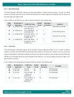
Pin No
B2B Connector1
Signal Name
FPGA Pin Name
FPGA
Bank
FPGA
Pin No
Signal Type/
Termination*
Description
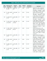
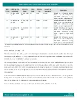
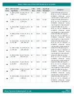
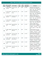
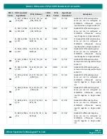
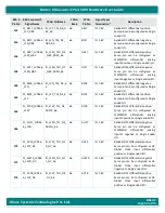
142
PL_AY27_LVDS6
5_L11N_A11_D2
7_GC
IO_L11N_T1U_
N9_GC_A11_D2
7_65
65
AY27
IO, 1.8V
Bank65 IO11 differential negative.
Same pin can be configured as GC Global
Clock Input differential positive or Single
ended I/O.
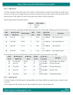
144
PL_AY26_LVDS6
5_L11P_A10_D2
6_GC
IO_L11P_T1U_
N8_GC_A10_D2
6_65
65
AY26
IO, 1.8V
Bank65 IO11 differential positive.
Same pin can be configured as GC Global
Clock Input differential positive or Single
ended I/O.
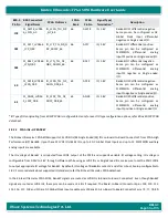
*IO Type of IOs originating from KU19P FPGA is configurable. Hence for exact IO type configuration options, refer Xilinx KU19P FPGA
datasheet.
2.7.3
Power Control Input
The Kintex Ult FPGA SOM works with 5V power input (VCC) from Board-to-Board Connector2 and generates all other
required powers internally On-SOM itself. SOM power can be enabled/disabled from the carrier board through SOM Power enable
pin in Board-to-Board Connector1. Also, in Board-to-Board Connector1, Ground pins are distributed throughout the connector for
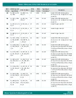
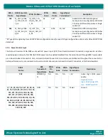
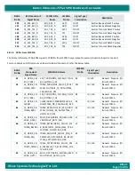
better performance. For more details on Power control & Ground pins on Board-to-Board Connector1, refer the below table.
B2B-1
Pin No
B2B
Connector1
Signal Name
FPGA
Pin
Name
FPGA
Bank
FPGA
Pin No
Signal Type/
Termination
Description
232
SOMPWR_E
N
NA
NA
NA
I, 5V
Active High SOM power
enable.
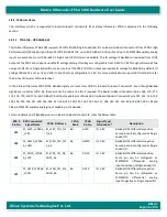
Important Note:
High
–
SOM power ON
Low
–
SOM Power OFF
1, 7, 13, 19, 25, 35, 41, 47, 53, 59, 61,
67, 73, 79, 85, 95, 101, 107, 113, 119,
121, 127, 133, 139, 145, 155, 161,
167, 173, 179, 181, 187, 193, 199,
205, 215, 221, 227, 233, 239, 2, 8, 20,
26, 36, 54, 60, 62, 68, 80, 86, 96, 102,
114, 120, 122, 140, 146, 156, 162,
174, 180, 182, 188, 200, 206, 216,
222, 234, 240
GND
NA
NA
NA
Power
Ground.


