REL0.1
Page 23 of 95
Kintex Ult FPGA SOM Hardware User Guide
iWave Systems Technologies Pvt. Ltd.
2.5
FPGA to CPU Interfaces
2.5.1
PCIex1 Gen2
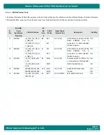
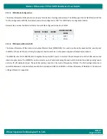
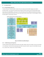
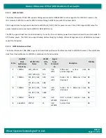
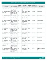
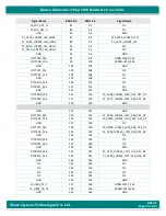
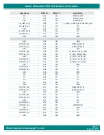
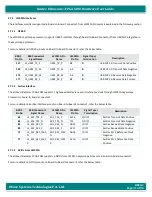
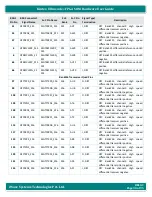
The Kintex Ult SOM supports Generation2 PCIex1 interface between LS1021A Processor and KU19P. Channel3 of KU19P
GTY Transceiver Bank228 is connected to LS1021A SERDES SD1 for PCIe interface.
Refer the below table for more details.
* Signal directions mentioned in table are based on LS1021A chip.
2.5.2
RGMII
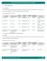
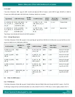
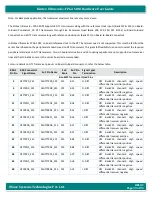
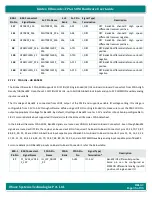
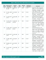
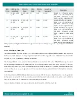
The Kintex Ult SOM supports RGMII interface between LS1021A Processor and KU19P through Ethernet Controller3
interface of LS1021A and PL HP Bank65 of KU19P.
Refer the below table for more details.
Signal Name
LS1021A Pin Name
LS1021A
Pin No
KU19P Pin
Name
KU19P Pin
No.
Signal Type/
Termination
*
Description
LS_SD1_RX0_P
SD1_RX0_P
AC10
MGTYTXP3_228 AF7
I, DIFF
SerDes Receive Data0
positive
LS_SD1_RX0_N
SD1_RX0_N
AB10
MGTYTXN3_228 AF6
I, DIFF
SerDes Receive Data0
negative
LS_SD1_TX0_P
SD1_TX0_P
W10
MGTYRXP3_228 AF2
O, DIFF
SerDes
Transmit
Data0 positive
LS_SD1_TX0_N
SD1_TX0_N
Y10
MGTYRXN3_228 AF1
O, DIFF
SerDes
Transmit
Data0 negative
LS_PERST0_PL_AR26(
EC2_RX_CLK)
EC2_RX_CLK/GPIO3
_26/USB2_DIR/FT
M2_QD_PHA
R1
IO_T3U_N12_PE
RSTN0_65
AR26
O, 1.8V
PCIe Reset input from
LS1021A to KU19P
Signal Name
LS1021A Pin Name
LS1021A
Pin No
KU19P Pin
Name
KU19P Pin
No.
Signal Type/
Termination
*
Description
LS_EC3_TXCLK_PL_BC
27_L6N_65
EC3_GTX_CLK/GPI
O4_01/EC2_TX_ER/
FTM3_CH0/EC3_TX
_CLK
V5
IO_L6N_T0U_N
11_AD6N_A21_
65
BC27
O, 1.8V
Transmit Clock Out
LS_EC3_TXD0_PL_BC2
6_L6P_65
EC3_TXD0/GPIO3_
31/TSEC_1588_PUL
SE_OUT2/FTM3_C
H4
W4
IO_L6P_T0U_N1
0_AD6P_A20_6
5
BC26
O, 1.8V
Transmit Data

