background image

UG121 Rev.0.00

Page 15 of 20

May 3, 2017

ISL71026MEVAL1Z

6. Typical Performance Curves

6.

Typical Performance Curves

Unless noted: VCC = 3.3V, D = 125kHz, Square Wave, 0 to VCC, 50% Duty Cycle, t

r

 = t

f

 ≤6ns, T

A

 = +25°C

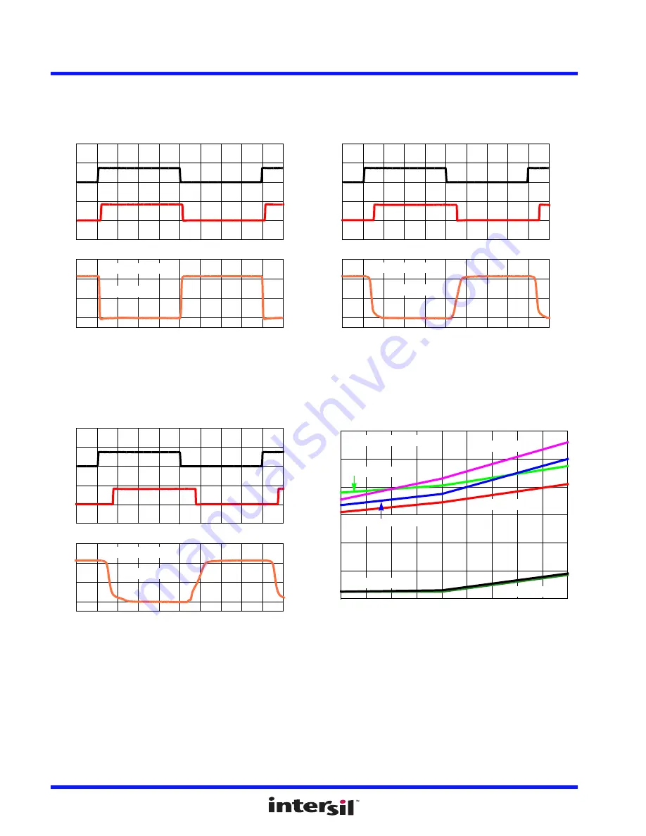
Figure 6.1

 Fast Driver and Receiver 
Waveforms 

Figure 6.2

Medium Driver and Receiver 
Waveforms 

Figure 6.3

Slow Driver and Receiver 
Waveforms 

Figure 6.4

Transmitter Propagation Delay 
and Skew vs Temperature at Fast 
Speed

0

4

0

TIME (1µs/DIV)

DRIV

E

R OUTPUT (

V)

D

R

IVE

R

 INPUT (

V)

4

0

1

2

3

RE

C

E

IV

ER OUTPUT (V

)

R

S

 = GND, R

D

 = 60Ω

CANH - CANL

R

D

0

4

0

TIME (1µs/DIV)

DRIVE

R

 OUTPUT (V)

DRIVER INP

UT

 (V

)

4

0

1

2

3

RECEIVER OUTPUT (V)

R

S

 = 10kΩ, R

D

 = 60Ω

CANH - CANL

R

D

0

4

0

TIME (1µs/DIV)

DRIVER OUTPUT (V)

DRIVER INP

U

T

 (V)

4

0

1

2

3

RECEIVE

R

 OU

T

P

U

T

 (V

)

R

S

 = 50kΩ, R

D

 = 60Ω

CANH - CANL

R

D

0

20

40

60

80

100

120

-55

-35

-15

5

25

45

65

85

105

125

TI

ME 

(ns

)

TEMPERATURE (°C)

R

S

 = GND, R

D

 = 60Ω

L TO H, V

CC

 = 3.6V

L TO H, V

CC 

= 3V

H TO L, V

CC 

= 3.6V

H TO L, V

CC

 = 3V

SKEW, V

CC 

= 3.6V

SKEW, V

CC 

= 3V

Summary of Contents for ISL71026MEVAL1Z

Page 1: ...User s Manual Rev 0 00 May 2017 ISL71026MEVAL1Z User s Manual Evaluation Board High Reliability Space ...

Page 2: ... the CAN controller and the CAN differential bus It can transmit and receive at bus speeds of up to 1Mbps It is designed to operate over a common mode range of 7V to 12V with a maximum of 120 nodes The device is capable of withstanding 20V on the CANH and CANL bus pins The part has various configurations of operation The evaluation board contains standard jumpers BNC connector banana connectors ca...

Page 3: ...optimized for the following conditions VCC 3V to 3 6V Data rate 1Mbps CAN bus termination resistance of 60Ω across the CANH and CANL differential signal lines Board temperature 25 C Figure 1 1 ISL71026MEVAL1Z Block Diagram 1 2 3 4 8 7 6 5 RS CANH CANL LBK D GND VCC R Tx DATA IN Rx DATA OUT CANH CANL ISL71026M 0 1µF VCC µController ...

Page 4: ...hat could have a wire soldered to it if you want to feed the digital output into a CAN controller board Control of the RS pin is through jumpers J5 J6 J7 and J8 located at middle left side of the evaluation board Only one of these jumper locations should have a jumper installed at any one time Putting the jumper at J5 will put the transceiver in the listen mode Putting the jumper at J6 will put th...

Page 5: ...ic level to the RS pin Jumper at J5 places the transceiver in a low current listen mode 2 3 3 LBK Pin When a high level is applied to the LBK pin the device enters the loop back state The transceiver CANH and CANL pins are disconnected from the bus The driver and receiver circuitry of the transceiver remains active to allow for diagnostic testing of the node Installing a jumper at position 1 to 2 ...

Page 6: ... ground jumper installed at this location will put the transceiver in high speed mode J9 Three pin jumper on the LBK pin Install jumper in upper position 1 to 2 to connect the LBK pin to VCC to put the part in loop back mode Remove jumper or put the jumper in the lower position 2 to 3 to connect LBK pin to ground for normal operation J10 Jumper location is not populated It needs to be populated if...

Page 7: ...Rise Fall Time 3 3V DC POWER SUPPLY ISL71026MEVAL1Z VCC GND J5 J7 J8 J6 R8 R7 R6 R9 TP7 TP8 TP3 TP4 R1 TP5 TP6 R10 R11 D CANH CANL R RS LOOP VCM TP9 GND TP11 GND TP2 GND GND TP1 J1 TP13 C2 U1 0V to 3 3V FUNCTION GENERATOR 125kHz SQUARE WAVE CH1 CH2 CH3 CH4 OSCILLOSCOPE TP3 TP7 TP8 TP4 CONNECT PROBES AT THE FOLLOWING D CANH CANL R 50Ω TEST POINTS ON THE EVALUATION BOARD ...

Page 8: ...e Channel 4 probe to the R pin by connecting the oscilloscope probe at TP4 on the evaluation board and the probe ground at TP2 4 Connect the function signal generator at the BNC connector labeled D on the evaluation board as shown in Figure 2 1 on page 6 Set the generator to output a 125kHz square wave 0V to 3 3V amplitude 50 duty cycle with a trise tfall 6ns Disable the generator output 5 Verify ...

Page 9: ...gure 4 2 on page 9 11 In medium speed mode RS 10kΩ tPLH should be around 520ns and no greater than 850ns tPHL should be around 460ns and no greater than 800ns tr should be around 400ns and no less than 200ns or greater than 780ns tf should be around 300ns and no less than 175ns or greater than 500ns 12 Move the jumper from J7 to J6 selects slow driver edges by connecting the RS pin to ground throu...

Page 10: ...Rev 0 00 Page 9 of 20 May 3 2017 ISL71026MEVAL1Z 4 Waveforms 4 Waveforms Figure 4 1 Oscilloscope Plot Fast Speed Waveforms and Measurements Figure 4 2 Oscilloscope Plot Medium Speed Waveforms and Measurements ...

Page 11: ...UG121 Rev 0 00 Page 10 of 20 May 3 2017 ISL71026MEVAL1Z 4 Waveforms Figure 4 3 Oscilloscope Plot Slow Speed Waveforms and Measurements ...

Page 12: ...UG121 Rev 0 00 Page 11 of 20 May 3 2017 ISL71026MEVAL1Z 5 PCB Layout Guidelines 5 PCB Layout Guidelines 5 1 Evaluation Board Figure 5 1 ISL71026MEVAL1Z Evaluation Board ...

Page 13: ...ISL71026MEVAL1Z 5 PCB Layout Guidelines UG121 Rev 0 00 Page 12 of 20 May 3 2017 5 2 Schematic Figure 5 2 ISL71026MEVAL1Z Circuit Schematic ...

Page 14: ...SS ROHS Keystone 575 4 1 ea U1 CAN BUS PART 14Ld TSSOP Intersil ISL71026MVZ 1 ea J9 CONN HEADER 1X3 BREAKAWY 1X36 2 54mm ROHS BERG FCI 68000 236HLF 4 ea J5 J6 J7 J8 CONN HEADER 1X2 RETENTIVE 2 54mm 0 230X0 120 ROHS BERG FCI 69190 202HLF 0 ea R2 R7 R8 R12 R13 RESISTOR SMD 0805 DNP TF ROHS 4 ea R1 R6 R10 R11 RES SMD 0805 0Ω 1 8W TF ROHS Yageo RC0805JR 070RL 1 ea R5 RES SMD 0805 10kΩ 1 8W 1 TF ROHS V...

Page 15: ...UG121 Rev 0 00 Page 14 of 20 May 3 2017 ISL71026MEVAL1Z 5 PCB Layout Guidelines 5 4 Board Layout Figure 5 3 Top Layer Figure 5 4 Bottom Layer Figure 5 5 Top Layer Silk Screen ...

Page 16: ...itter Propagation Delay and Skew vs Temperature at Fast Speed 0 4 0 TIME 1µs DIV DRIVER OUTPUT V DRIVER INPUT V 4 0 1 2 3 RECEIVER OUTPUT V RS GND RD 60Ω CANH CANL R D 0 4 0 TIME 1µs DIV DRIVER OUTPUT V DRIVER INPUT V 4 0 1 2 3 RECEIVER OUTPUT V RS 10kΩ RD 60Ω CANH CANL R D 0 4 0 TIME 1µs DIV DRIVER OUTPUT V DRIVER INPUT V 4 0 1 2 3 RECEIVER OUTPUT V RS 50kΩ RD 60Ω CANH CANL R D 0 20 40 60 80 100 ...

Page 17: ...0 400 500 600 700 800 55 35 15 5 25 45 65 85 105 125 RS 10kΩ RD 60Ω L TO H VCC 3 6V L TO H VCC 3V H TO L VCC 3 6V H TO L VCC 3V SKEW VCC 3 6V SKEW VCC 3V TIME ns TEMPERATURE C 0 200 400 600 800 1000 1200 55 35 15 5 25 45 65 85 105 125 RS 10kΩ RD 60Ω L TO H VCC 3 6V L TO H VCC 3V H TO L VCC 3 6V H TO L VCC 3V SKEW VCC 3 6V SKEW VCC 3V 20 25 30 35 40 45 50 55 60 55 35 15 5 25 45 65 85 105 125 TIME n...

Page 18: ...UG121 Rev 0 00 Page 17 of 20 May 3 2017 ISL71026MEVAL1Z 7 Revision History 7 Revision History Rev Date Description Page Summary 0 00 May 3 2017 Initial release ...

Page 19: ...re intended for developers skilled in the art designing with Renesas products You are solely responsible for 1 selecting the appropriate products for your application 2 designing validating and testing your application and 3 ensuring your application meets applicable standards and any other safety security or other requirements These resources are subject to change without notice Renesas grants yo...

Page 20: ...20 ISL71026MEVAL1Z UG121 ...

Page 21: ...Mouser Electronics Authorized Distributor Click to View Pricing Inventory Delivery Lifecycle Information Renesas Electronics ISL71026MEVAL1Z ...

Reviews: