background image

2.3.2. Clocking Scheme

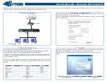
Figure 16.

Parallel Loopback with Simplex Mode

F-tile PMA/

FEC Direct

PHY IP (TX)

SDI II

(TX)

TX PLL Refclock
System PLL Refclock

RX Coreclock/DR Clocks

RX CDR Refclock

TX PLL/RX CDR Link Clock

System PLL Output Link Clock

TX/RX Transceiver Clkout

TX/RX Transceiver Clkout2

Top

Rx Top

TX Top

Loopback

FIFO

SDI RX Sys

Loopback Top

SDI TX Sys

SDI F-tile

PHY Adapter

F-tile PMA/

FEC Direct

PHY IP (RX)

SDI II

(RX)

SDI F-tile

PHY Adapter

Device_init

GPIO Clock

TX PLL

Ref Clock

SysPLL

Ref Clock

RX CDR

Ref Clock

Reference

and System

PLL Clocks IP

2. Design Example Detailed Description

710496 | 2022.01.28

F-Tile SDI II Intel

®

 Agilex

 FPGA IP Design Example User Guide

Send Feedback

22

Summary of Contents for F-Tile SDI II Intel Agilex

Page 1: ...F Tile SDI II Intel Agilex FPGA IP Design Example User Guide Updated for Intel Quartus Prime Design Suite 21 4 IP Version 19 2 0 Online Version Send Feedback ID 710496 Version 2022 01 28...

Page 2: ...le Detailed Description 13 2 1 Features 13 2 2 Hardware and Software Requirements 14 2 3 Functional Description 15 2 3 1 Design Components 19 2 3 2 Clocking Scheme 22 2 4 Simulation 27 2 4 1 Testbench...

Page 3: ...he generated files for the design examples 710496 2022 01 28 Send Feedback Intel Corporation All rights reserved Intel the Intel logo and other Intel marks are trademarks of Intel Corporation or its s...

Page 4: ...l loopback design simulation mentor synopsys testbench xcelium reset_releaseipgeneratedfolder reset_release ip jtag sdc sim_setup_gen sh Table 1 Other Generated Files in RTL Folder Folders Files vid_p...

Page 5: ...p sv rx_checker sdi_ii_tb_rx_checker v rx_checker tb_data_compare v rx_checker tb_dual_link_sync v rx_checker tb_fifo_line_test v rx_checker tb_frame_locked_test sv rx_checker tb_ln_check v rx_checker...

Page 6: ...gilex device family and select the desired device 2 In the IP Catalog locate and double click SDI II Intel FPGA IP The IP Parameter Editor window appears 3 Specify a top level name for your custom IP...

Page 7: ...example design simulation follow these steps 1 Generate the necessary simulation setup files a Using GUI method i Open the Intel Quartus Prime Project in Intel Quartus Prime directory ii Run Support...

Page 8: ...sh 2 Go to simulation folder 3 Go to the desired simulator folder and run the simulation script a ModelSim SE or Questa FE Bring up the simulator GUI change directory to mentor folder and type do ment...

Page 9: ...r J1 12G In or a video analyzer 5 Ensure all the switches on the development kit are in their default position per Agilex I series SoC Development Kit User Guide 6 After the compilation completes open...

Page 10: ...itching between fractional frame rate and integer frame rate video format You must press the push button PB0 to trigger a device LMK03328 power cycling through the PDN pin every time you change the ju...

Page 11: ...on testbench Synthesis On Turns on this option to generate necessary files forIntel Quartus Prime compilation and hardware demo This option is greyed out and set to always Enabled This is because synt...

Page 12: ...argeted device All the pins assignment has been set accordingly to the development kit Custom Development Kit This option allows the design example to be tested on a third party development kit with I...

Page 13: ...ectations are forward looking statements These statements are based on current expectations and involve many risks and uncertainties that could cause actual results to differ materially from those exp...

Page 14: ...SDI II TX SDI II RX SDI F tile PHY Adapter Device_init Common components for TX RX only design Note Refer to Clocking Scheme on page 22 for the Reference and System PLL Clocks IP connections 2 2 Hardw...

Page 15: ...A IP design example fail to compile at the Support Logic Generation stage 2 3 Functional Description The SDI II Intel FPGA IP core design example supports the following simplex and duplex transceiver...

Page 16: ...erence and System PLL Clocks IP SDI F tile PHY Adapter F tile PMA FEC Direct PHY IP RX F tile PMA FEC Direct PHY IP TX Device_init SDI II RX SDI II TX Note Refer to Clocking Scheme on page 22 for the...

Page 17: ...PLL Clocks IP SDI F tile PHY Adapter Device_init F tile PMA FEC Direct PHY IP RX F tile PMA FEC Direct PHY IP TX SDI II Duplex Note Refer to Clocking Scheme on page 22 for the Reference and System PLL...

Page 18: ...ystem PLL Clocks IP Video Pattern Generator SDI F tile PHY Adapter F tile PMA FEC Direct PHY IP TX F tile PMA FEC Direct PHY IP RX SDI II TX SDI II RX SDI F tile PHY Adapter Device_init Note Refer to...

Page 19: ...I F tile PHY Adapter Device_init F tile PMA FEC Direct PHY IP RX F tile PMA FEC Direct PHY IP TX SDI II Duplex Note Refer to Clocking Scheme on page 22 for the Reference and System PLL Clocks IP conne...

Page 20: ...h of parallel data between transceiver and SDI core as well as to transfer the data between these two clock domains Table 7 Loopback Top Components Component Description Loopback FIFO This module cont...

Page 21: ...in operation The module also includes a reset delay block to further delay the signal status from the IP for a safer operation For more information refer to Intel Agilex Reset Release Intel FPGA IP in...

Page 22: ...Transceiver Clkout TX RX Transceiver Clkout2 Top Rx Top TX Top Loopback FIFO SDI RX Sys Loopback Top SDI TX Sys SDI F tile PHY Adapter F tile PMA FEC Direct PHY IP RX SDI II RX SDI F tile PHY Adapter...

Page 23: ...Clocks IP GPIO Clock TX PLL Ref Clock SysPLL Ref Clock RX CDR Ref Clock TX PLL Refclock System PLL Refclock RX Coreclock RX CDR Refclock TX PLL RX CDR Link Clock System PLL Output Link Clock TX RX Tr...

Page 24: ...to Avalon Master Bridge Pattern Ctrl SDI RX Sys SDI TX Sys Video Pattern Generator SDI F tile PHY Adapter F tile PMA FEC Direct PHY IP TX F tile PMA FEC Direct PHY IP RX SDI II TX SDI II RX SDI F tile...

Page 25: ...ck System PLL Output Link Clock TX RX Transceiver Clkout TX RX Transceiver Clkout2 2 3 2 1 Clocking Scheme Component Table 10 Clocking Scheme Component Diagram label Description TX PLL refclock TX PLL...

Page 26: ...clock set to 148 5 MHz regardless of the GUI option because of the development kit s default limited clock frequency option TX PLL RX CDR link clock Output ports from Reference and System PLL Clocks...

Page 27: ...EC Direct PHY IP TX SDI II TX RX Top SDI F tile PHY Adapter F tile PMA FEC Direct PHY IP RX SDI II RX Video Pattern Generator Testbench Control Reference and System PLL Clocks IP SDI Rx Sys Note Refer...

Page 28: ...ls the test sequence of the simulation and generates the necessary stimulus signals to the TX and video pattern generator blocks TX checker This checker verifies if the TX serial data contains a valid...

Page 29: ...nt Kit User LEDs Figure and the D3 D5 LED status and its video standard on Agilex I series SoC Dev Kit Table After verifying that RX is working fine connect an SDI signal analyzer to the transmitter o...

Page 30: ...110 12G 10 bit Multiplex Type 2 111 12G 10 bit Multiplex Type 1 2 4 4 Signal Table 15 Top Level Signals Signal Name Direction Width Description On board Oscillators clk_a_12c_fgt_p_7 Input 1 156 25 M...

Page 31: ...be set to 1 Table 17 RX top TX top Du top signals Signal Name Direction Width Description Clocks system_pll_clk Input 1 System PLL output clock This port must be connected to the system PLL output po...

Page 32: ...asserts this signal when the horizontal blanking interval is active rx_vid_vsync Output Vertical blanking interval timing signal The receiver asserts this signal when the vertical blanking interval is...

Page 33: ...sdi_tx_vpid_byte3 Input 8 N sdi_tx_vpid_byte4 Input 8 N sdi_tx_vpid_byte1_b Input 8 N sdi_tx_vpid_byte2_b Input 8 N sdi_tx_vpid_byte3_b Input 8 N sdi_tx_vpid_byte4_b Input 8 N sdi_tx_datavalid Output...

Page 34: ...byte1_b Output 8 N sdi_rx_vpid_byte2_b Output 8 N sdi_rx_vpid_byte3_b Output 8 N sdi_rx_vpid_byte4_b Output 8 N sdi_rx_vpid_checksum _error_b Output N sdi_rx_vpid_valid_b Output N Transceiver Interfac...

Page 35: ...sdi_rx_dataout_valid Input 1 Data valid signal generated from SDI RX core sdi_rx_std Input 3 Received video standard from SDI RX core sdi_rx_trs Input N Receiver output signal from SDI core that indic...

Page 36: ...ted to sdi_tx_datavalid signal from TX Du top patho Input 1 Enable this signal to generate pathological pattern blank Input 1 Enable this signal to generate black signal no_color Input 1 Enable this s...

Page 37: ...4_b Output 8 N Payload ID output signal to be connected to sdi_tx_vpid_byte4_b input signal on TX Du top line_f0 Output 11 N Line number output signal to be inserted with Payload ID This signal must b...

Page 38: ...es device has finished its initialization stage after a programmable delay which is determined by CNTR_BITS parameter Note CNTR_BITS parameter determines the bit width of the delay counter Default val...

Page 39: ...cts to current specifications in accordance with Intel s standard warranty but reserves the right to make changes to any products and services at any time without notice Intel assumes no responsibilit...

Reviews: