January 2007
201
Intel
®
855GME Chipset and Intel
®
6300ESB ICH Embedded Platform Design Guide
Intel
®
6300ESB Design Guidelines
Using the assumed six layer stack-up, the AC’97 interface may be routed using 5 mil traces with
10 mil spacing between the traces. Maximum length between the 6300ESB and the CODEC/CNR
is 14 inches. This assumes that a CNR riser card implements its audio solution with a maximum
trace length of six inches for the AC-link. The CNR and mother board target trace impedance
should be Z
0
= 55
Ω
± 10% dependant on platform stackup described in
.
Clocking is provided from the primary codec on the link via AC_BIT_CLK, and is derived from a
24.576 MHz crystal or oscillator. Refer to the primary codec vendor for crystal or oscillator
requirements. AC_BIT_CLK is a 12.288 MHz clock driven by the primary codec to the digital
controller (6300ESB) and to any other codec present. That clock is used as the time base for
latching and driving data.
The 6300ESB supports wake on ring from S1-S5 through the AC’97 link. The codec asserts
AC_SDIN to wake the system. To provide wake capability and/or caller ID, standby power must be
provided to the modem codec.
The 6300ESB has pull-downs/pull-ups that are always enabled. This will keep the link from
floating when the AC-link is off, or there are no codecs present.
When the Shut-off bit is not set, it implies that there is a codec on the link. Therefore,
AC_BIT_CLK and AC_SDOUT will be driven by the codec and the 6300ESB, respectively.
However, AC_SDIN0, AC_SDIN1 and AC_SDIN2 may not be driven. When the link is enabled,
the assumption may be made that there is at least one codec.
Note:
A 15 pF cap to Gnd should replace an unpopulated motherboard codec for the CLK and
SDATA_IN lines to reduce reflection and improve signal quality.
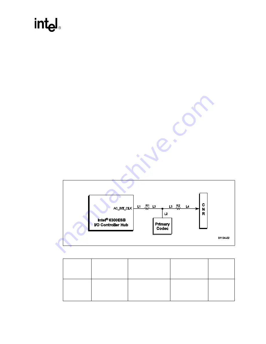
Figure 100.
6300ESB AC'97 – AC_BIT_CLK Topology
Table 76.
AC’97 AC_BIT_CLK Routing Summary
Trace
Impedance
AC’97 Routing
Requirements
Trace Lengths
Series Termination
Resistance
AC_BIT_CLK
Signal
Length
Matching
55
Ω
± 10%
5 mil width, 10 mil
spacing (based on
stackup assumptions
in
)
L1 = 3 to 8 inches
L2 = 0.1 to 0.5inches
L3 = 0.1 to 0.5 inches
L4 = 3 to 6 inches
R1 = 34.2
Ω
- 37.8
Ω
R2 = R1
(Optional 0
Ω
resistor for debug
purposes only).
N/A
Summary of Contents for 6300ESB ICH
Page 24: ...24 Intel 855GME Chipset and Intel 6300ESB ICH Embedded Platform Design Guide Introduction...
Page 102: ...102 Intel 855GME Chipset and Intel 6300ESB ICH Embedded Platform Design Guide...
Page 122: ...122 Intel 855GME Chipset and Intel 6300ESB ICH Embedded Platform Design Guide...
Page 190: ...190 Intel 855GME Chipset and Intel 6300ESB ICH Embedded Platform Design Guide Hub Interface...
Page 318: ...318 Intel 855GME Chipset and Intel 6300ESB ICH Embedded Platform Design Guide Layout Checklist...


