


S6SAP413A00SA1001 Power Solution for FPGA Evaluation Kit Operation Guide, Doc. No. 002-08725 Rev. *B
8
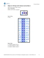
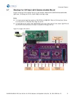
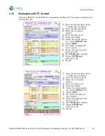
2. Pin Description
2.1
Input/Output Pin Descriptions
Figure 2-1. Input/Output Pin Descriptions
Component
Input or Output
Description
VIN
Input
Power supply terminal of DC/DC system / MB39C504
PGND
-
Power ground terminal
VOUT11
Output
Output of MB39C504
PGND11
-
Power ground terminal of MB39C504
VOUT11
Output
Output of MB39C504
PGND21
-
Power ground terminal of MB39C504
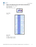
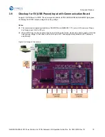
VOUT21
Output
Vo1 output of S6AP413A
VOUT22
Output
Vo2 output of S6AP413A
VOUT23
Output
Vo3 output of S6AP413A
VOUT24
Output
Vo4 output of S6AP413A
PGND22
-
Power ground terminal of S6AP413A
VOUT31
Output
Vo1 output of MB39C031
VOUT32
Output
Vo2 output of MB39C031
VOUT3L
Output
LDO output of MB39C031
PGND31
-
Power ground terminal of MB39C031


