


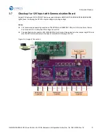
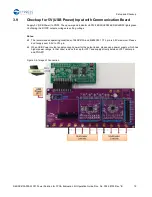
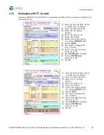

Pin Description
S6SAP413A00SA1001 Power Solution for FPGA Evaluation Kit Operation Guide, Doc. No. 002-08725 Rev. *B
9
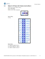
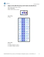
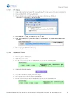
2.2
Jumper, Switch Descriptions
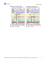
Figure 2-2. Jumper, Switch Descriptions
Jumper,
Switch
Description
Initial
setting
JP14
Short VIN terminal and EN1 pin of MB39C504
Pattern Short
JP02
Short PWRGD21 terminal and PWRGD31
Pattern Short
JP03
Short PWRGD24 terminal and PWRGD32
Pattern Short
JP21
Short CTLM pin of S6AP413A6B and VIN_5V pin
Pattern Short
JP31
Short CTLM pin of MB39C031 (142)and VIN_5V pin
Pattern Short
CTL24
CTL4 pin of S6AP413A
-
CTL23
CTL3 pin of S6AP413A
-
CTL22
CTL2 pin of S6AP413A
-
CTL21
CTL1 pin of S6AP413A
-
CTL3L
CTL3 pin of MB39C031
-
CTL32
CTL2 pin of MB39C031
-
CTL31
CTL1 pin of MB39C031
-
EN1
EN pin of MB39C504
-
SLP1
SLP_N pin of MB39C504
-
CTL2M
CTLM pin of S6AP413A
-
CTL3M
CTLM pin of MB39C031
-
ADDS3
ADDS pin of MB39C031
-
GND
GND terminal
-
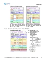
PWRGD21a
PG1 pin of S6AP413A
-
PWRGD22a
PG2 pin of S6AP413A
-
PWRGD24
PG4 pin of S6AP413A
-
VIN_5Va
Input terminal of S6AP413A6B and MB39C031
-
PWRGD22b
PG2 pin of S6AP413A
-
PWRGD21b
PG1 pin of S6AP413A
-
VIN_5Vb
Input terminal of S6AP413A6B and MB39C031
-
PWRGD11
PWRGD pin of MB39C504
-
PWRGD23
PG3 pin of S6AP413A
-
PWRGD3L
PGL pin of MB39C031
-
PWRGD31
PG1 pin of MB39C031
-
PWRGD32
PG2 pin of MB39C031
-
ERR3
ERR pin of MB39C031
-
CN01
Connector for communication board
-
CN02
Jack for AC adopter
-
CN03
USB connector for power supply
-


