


WAFER-ULT/ULT2-i1 3.5" SBC
Page 22
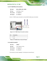
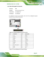
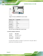
Figure 3-4: Audio Connector Location
Pin Description Pin Description
1
LINEOUT1R
2 LINE1_R
3 AUD_GND 4 AUD_GND
5
LINEOUT1L
6 LINE1_L
7 AUD_GND 8 AUD_GND
9 FMIC1_R 10
FMIC1_L
Table 3-5: Audio Connector Pinouts
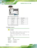
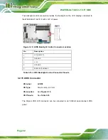
3.2.4 Battery Connector
CAUTION:
Risk of explosion if battery is replaced by an incorrect type. Only
certified engineers should replace the on-board battery.
Dispose of used batteries according to instructions and local
regulations.
CN Label:
CN4
CN Type:
2-pin wafer, p=1.25 mm
CN Location:
CN Pinouts:
Summary of Contents for WAFER-ULT-i1
Page 9: ...WAFER ULT ULT2 i1 3 5 SBC Page ix E WATCHDOG TIMER 144 F HAZARDOUS MATERIALS DISCLOSURE 147...
Page 16: ...WAFER ULT ULT2 i1 3 5 SBC Page 1 Chapter 1 1 Introduction...
Page 21: ...WAFER ULT ULT2 i1 3 5 SBC Page 6 Figure 1 3 WAFER ULT ULT2 i1 Dimensions mm...
Page 26: ...WAFER ULT ULT2 i1 3 5 SBC Page 11 Chapter 2 2 Packing List...
Page 31: ...WAFER ULT ULT2 i1 3 5 SBC Page 16 Chapter 3 3 Connectors...
Page 64: ...WAFER ULT ULT2 i1 3 5 SBC Page 49 Chapter 4 4 Installation...
Page 88: ...WAFER ULT ULT2 i1 3 5 SBC Page 73 Chapter 5 5 BIOS...
Page 127: ...WAFER ULT ULT2 i1 3 5 SBC Page 112 6 Software Drivers Chapter 6...
Page 147: ...WAFER ULT ULT2 i1 3 5 SBC Page 132 Appendix A A Regulatory Compliance...
Page 149: ...WAFER ULT ULT2 i1 3 5 SBC Page 134 Appendix B B BIOS Options...
Page 152: ...WAFER ULT ULT2 i1 3 5 SBC Page 137 Appendix C C Terminology...
Page 156: ...WAFER ULT ULT2 i1 3 5 SBC Page 141 Appendix D D Digital I O Interface...
Page 159: ...WAFER ULT ULT2 i1 3 5 SBC Page 144 Appendix E E Watchdog Timer...
Page 162: ...WAFER ULT ULT2 i1 3 5 SBC Page 147 Appendix F F Hazardous Materials Disclosure...