WAFER-OT-Z650/Z670 3.5" Motherboard
Page 20
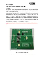
Figure 3-7: LVDS Connector Location
Pin Description
Pin Description
1 GND
2 GND
3 AY0+
4 AY0-
5 AY1+
6 AY1-
7 AY2+
8 AY2-
9 AYCLK+ 10
AYCLK-
11 AY3+
12 AY3-
13 GND
14 GND
15 NC
16 NC
17 LCDVCC 18 LCDVCC
19 LCDVCC 20 LCDVCC
Table 3-8: LVDS Connector Pinouts
3.2.7 Power & HDD LED Connector
CN Label:
CN1
CN Type:
6-pin wafer
CN Location:
CN Pinouts:
The LED connector connects to an HDD indicator LED and a power LED on the system
chassis to inform the user about HDD activity and the power on/off status of the system.
Summary of Contents for WAFER-OT-Z650
Page 14: ...WAFER OT Z650 Z670 3 5 Motherboard Page 1 Chapter 1 1 Introduction ...
Page 21: ...WAFER OT Z650 Z670 3 5 Motherboard Page 8 Chapter 2 2 Packing List ...
Page 25: ...WAFER OT Z650 Z670 3 5 Motherboard Page 12 Chapter 3 3 Connectors ...
Page 44: ...WAFER OT Z650 Z670 3 5 Motherboard Page 31 Chapter 4 4 Installation ...
Page 62: ...WAFER OT Z650 Z670 3 5 Motherboard Page 49 Chapter 5 5 BIOS ...
Page 82: ...WAFER OT Z650 Z670 3 5 Motherboard Page 69 6 Software Drivers Chapter 6 ...
Page 102: ...WAFER OT Z650 Z670 3 5 Motherboard Page 89 Appendix A A BIOS Options ...
Page 104: ...WAFER OT Z650 Z670 3 5 Motherboard Page 91 Appendix B B One Key Recovery ...
Page 112: ...WAFER OT Z650 Z670 3 5 Motherboard Page 99 Figure B 5 Partition Creation Commands ...
Page 146: ...WAFER OT Z650 Z670 3 5 Motherboard Page 133 Appendix C C Terminology ...
Page 150: ...WAFER OT Z650 Z670 3 5 Motherboard Page 137 Appendix D D Watchdog Timer ...
Page 153: ...WAFER OT Z650 Z670 3 5 Motherboard Page 140 Appendix E E Hazardous Materials Disclosure ...