background image


WAFER-CV-D25501/N26001 3.5" SBC

Page 52 


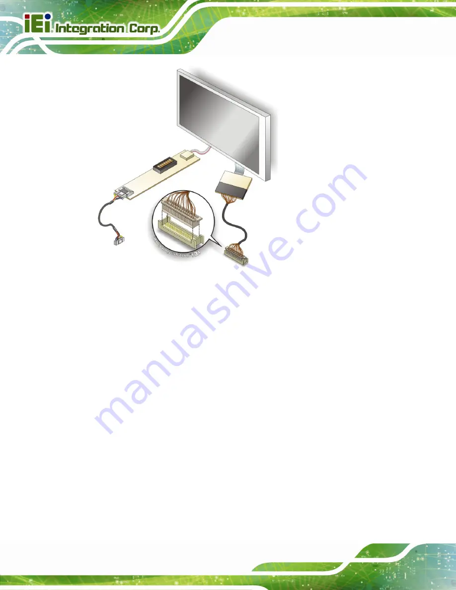
Figure 4-10: LVDS Connector 

Step 3: 

Locate the backlight inverter connector.

 The locations of the backlight 

inverter connectors are shown in 

Chapter 3

Step 4: 

Connect backlight connector

. Connect the backlight connector to the driver 

TFT LCD PCB as shown in 

Figure 4-11

. When inserting the cable connector, 

make sure the pins are properly aligned. 

Summary of Contents for WAFER-CV-N26001

Page 1: ...01 N26001 3 5 SBC Page i User Manual 3 5 SBC with Intel Atom D2550 N2600 Processor DDR3 VGA Dual LVDS Dual PCIe GbE USB 2 0 PCIe Mini SATA 3Gb s Audio and RoHS MODEL WAFER CV D25501 N26001 Rev 1 05 Oc...

Page 2: ...ector August 27 2015 1 04 Updated Section 1 4 Dimensions Updated Section 4 5 Chassis Installation December 11 2012 1 03 Added CN6 connector information 23 November 2012 1 02 Updated the note for the I...

Page 3: ...mages arising out of the use or inability to use the product or documentation even if advised of the possibility of such damages This document contains proprietary information protected by copyright A...

Page 4: ...AUTION Cautionary messages should be heeded to help reduce the chance of losing data or damaging the product NOTE These messages inform the reader of essential but non critical information These messa...

Page 5: ...ECTORS 13 3 1 PERIPHERAL INTERFACE CONNECTORS 14 3 1 1 WAFER CV D25501 N26001 Layout 14 3 1 2 Peripheral Interface Connectors 15 3 1 3 External Interface Panel Connectors 16 3 2 INTERNAL PERIPHERAL CO...

Page 6: ...s 36 3 3 4 VGA Connector 36 4 INSTALLATION 38 4 1 ANTI STATIC PRECAUTIONS 39 4 2 INSTALLATION CONSIDERATIONS 39 4 3 SO DIMM INSTALLATION 41 4 4 JUMPER SETTINGS 42 4 4 1 AT ATX Power Selection Jumper 4...

Page 7: ...nfiguration 69 5 3 5 USB Configuration 70 5 3 6 F81866 Super IO Configuration 71 5 3 6 1 Serial Port n Configuration 71 5 3 7 F81866 H W Monitor 75 5 3 7 1 Smart Fan Mode Configuration 76 5 3 8 Serial...

Page 8: ...6 AUDIO DRIVER INSTALLATION 101 A REGULATORY COMPLIANCE 104 B BIOS OPTIONS 106 C TERMINOLOGY 109 D DIGITAL I O INTERFACE 113 D 1 INTRODUCTION 114 D 2 ASSEMBLY LANGUAGE SAMPLE 1 115 D 3 ASSEMBLY LANGUA...

Page 9: ...tor Location 23 Figure 3 10 LVDS1 Connector Location 24 Figure 3 11 LVDS2 Connector Location 25 Figure 3 12 LVDS2 Backlight Control Connector Location 26 Figure 3 13 PCIe Mini Card Slot Locations 27 F...

Page 10: ...at an Angle 56 Figure 4 17 Secure the Half size PCIe Mini Card 56 Figure 4 18 SATA Drive Cable Connection 57 Figure 4 19 Single RS 232 Cable Installation 58 Figure 4 20 Keyboard mouse Y cable Connecti...

Page 11: ...WAFER CV D25501 N26001 3 5 SBC Page xi Figure 6 18 Audio Driver Installation Complete 103...

Page 12: ...Table 3 9 Fan Connector Pinouts 22 Table 3 10 Keyboard Mouse Connector Pinouts 23 Table 3 11 LVDS1 Connector Pinouts 24 Table 3 12 LVDS2 Connector Pinouts 25 Table 3 13 LVDS2 Backlight Control Connect...

Page 13: ...le 4 2 AT ATX Power Selection Jumper Settings 43 Table 4 3 Clear CMOS Jumper Settings 43 Table 4 4 LVDS1 Voltage Selection Jumper Settings 44 Table 4 5 LVDS2 Voltage Selection Jumper Settings 45 Table...

Page 14: ...r IO Configuration 71 BIOS Menu 9 Serial Port n Configuration Menu 71 BIOS Menu 10 F81866 H W Monitor 75 BIOS Menu 11 Smart Fan Mode Configuration 77 BIOS Menu 12 Serial Port Console Redirection 78 BI...

Page 15: ...WAFER CV D25501 N26001 3 5 SBC Page 1 Chapter 1 1 Introduction...

Page 16: ...isplay output and comes with two LVDS connectors supporting 24 bit or 18 bit LVDS screens Maximum six USB ports two SATA 3Gb s connectors two PCIe Mini card slots four COM ports and one audio connecto...

Page 17: ...WAFER CV D25501 N26001 3 5 SBC Page 3 1 3 Connectors The connectors on the WAFER CV D25501 N26001 are shown in the figure below Figure 1 2 Connectors...

Page 18: ...WAFER CV D25501 N26001 3 5 SBC Page 4 1 4 Dimensions The main dimensions of the WAFER CV D25501 N26001 are shown in the diagram below...

Page 19: ...WAFER CV D25501 N26001 3 5 SBC Page 5 Figure 1 3 WAFER CV D25501 N26001 Dimensions mm...

Page 20: ...WAFER CV D25501 N26001 3 5 SBC Page 6 1 5 Data Flow 5Figure 1 4 shows the data flow between the system chipset the CPU and other components installed on the motherboard Figure 1 4 Data Flow Diagram...

Page 21: ...s driven by the Chrontel CH7511 DP to LVDS converter 24 bit single channel LVDS1 with up to 1440x900 resolution 18 bit single channel LVDS1 with up to 1366x768 resolution Display 24 bit dual channel L...

Page 22: ...pply 12 V only AT and ATX support One internal 4 pin 2x2 power connector Power Consumption 12V 1 53 A 1 86 GHz Intel Atom D2550 with 1 GB 1066 MHz DDR3 SO DIMM memory 12V 1 15 A 1 6 GHz Intel Atom N26...

Page 23: ...WAFER CV D25501 N26001 3 5 SBC Page 9 Chapter 2 2 Packing List...

Page 24: ...ischarge Self grounding Touch a grounded conductor every few minutes to discharge any excess static buildup Use an anti static pad When configuring any circuit board place it on an anti static mat Onl...

Page 25: ...chased from or contact an IEI sales representative directly by sending an email to 32sales ieiworld com3 The WAFER CV D25501 N26001 is shipped with the following components Quantity Item and Part Numb...

Page 26: ...ry CD 1 Utility CD 1 Quick Installation Guide Table 2 1 Packing List 2 4 Optional Items The following are optional components which may be separately purchased Item and Part Number Image Dual USB cabl...

Page 27: ...WAFER CV D25501 N26001 3 5 SBC Page 13 Chapter 3 3 Connectors...

Page 28: ...5 SBC Page 14 3 1 Peripheral Interface Connectors This chapter details all the jumpers and connectors 3 1 1 WAFER CV D25501 N26001 Layout The figure below shows all the connectors and jumpers Figure 3...

Page 29: ...header DIO1 Fan connectors 3 pin wafer CPU_FAN1 SYS_FAN2 Keyboard and mouse connector 6 pin wafer KB_MS1 LVDS connectors 20 pin 30 pin crimp LVDS1 LVDS2 LVDS2 backlight control connector 6 pin wafer...

Page 30: ...onnector Male DB 9 COM1 VGA connector 15 pin female VGA1 Table 3 2 Rear Panel Connectors 3 2 Internal Peripheral Connectors The section describes all of the connectors on the WAFER CV D25501 N26001 3...

Page 31: ...n Molex power connector CN Location See Figure 3 3 CN Pinouts See Table 3 4 The ATX power connector connects to an ATX power supply Figure 3 3 12 V Power Connector Location Pin Description 1 GND 2 GND...

Page 32: ...n Pin Description Pin Description 1 Line out_R 2 Line in_R 3 AUD_GND 4 AUD_GND 5 Line out _L 6 Line in _L 7 AUD_GND 8 AUD_GND 9 MIC1_R 10 MIC1_L Table 3 5 Audio Connector Pinouts 3 2 4 Backlight Inver...

Page 33: ...V 4 GROUND 5 LCD_BKLEN Table 3 6 Backlight Inverter Connector Pinouts 3 2 5 Battery Connector CAUTION Risk of explosion if battery is replaced by an incorrect type Only certified engineers should repl...

Page 34: ...n the time when power is turned off Figure 3 6 Battery Connector Location Pin Description 1 Battery 2 GND Table 3 7 Battery Connector Pinouts 3 2 6 Digital Input Output DIO Connector CN Label DIO1 CN...

Page 35: ...1 GND 2 VCC 3 Output 3 4 Output 2 5 Output 1 6 Output 0 7 Input 3 8 Input 2 9 Input 1 10 Input 0 Table 3 8 Digital I O Connector Pinouts 3 2 7 Fan Connectors CN Label CPU_FAN1 SYS_FAN1 CN Type 3 pin w...

Page 36: ...Speed Detect Table 3 9 Fan Connector Pinouts 3 2 8 Keyboard Mouse Connector CN Label KB_MS1 CN Type 6 pin wafer CN Location See Figure 3 9 CN Pinouts See Table 3 10 The keyboard and mouse connector c...

Page 37: ...KB DATA 2 MS DATA 3 MS CLK 4 KB DATA 5 KB CLK 6 GROUND Table 3 10 Keyboard Mouse Connector Pinouts 3 2 9 LVDS1 Connector CN Label LVDS1 CN Type 20 pin crimp CN Location See Figure 3 10 CN Pinouts See...

Page 38: ...TA2 8 LVDS_DATA2 9 LVDS_CLK 10 LVDS_CLK 11 LVDS_DATA3 12 LVDS_DATA3 13 GND 14 GND 15 LDDC_DATA 16 LDDC_CLK 17 VCC_LCD 18 VCC_LCD 19 VCC_LCD 20 VCC_LCD Table 3 11 LVDS1 Connector Pinouts 3 2 10 LVDS2 C...

Page 39: ...LVDS_DATA1 6 LVDS_DATA1 7 LVDS_DATA2 8 LVDS_DATA2 9 LVDS_CLK1 10 LVDS_CLK1 11 LVDS_DATA3 12 LVDS_DATA3 13 GND 14 GND 15 LVDS_DATA4 16 LVDS_DATA4 17 LVDS_DATA5 18 LVDS_DATA5 19 LVDS_DATA6 20 LVDS_DATA6...

Page 40: ...nnector Location Function Pin Description 1 PWRDN Panel power button 2 GND 3 BLUP Panel brightness 4 GND 5 BLDN Panel brightness 6 GND Table 3 13 LVDS2 Backlight Control Connector Pinouts 3 2 12 PCIe...

Page 41: ...Pin Description Pin Description 1 PCIE_WAKE 2 VCC3 3 N C 4 GND 5 N C 6 1 5V 7 N C 8 N C 9 GND 10 N C 11 PCIE_CLK 12 N C 13 PCIE_CLK 14 N C 15 GND 16 N C 17 N C 18 GND 19 N C 20 N C 21 GND 22 PCIRST 23...

Page 42: ...52 VCC3 Table 3 14 PCIe Mini Card Slot Pinouts 3 2 13 Power HDD LED Connector CN Label CN2 CN Type 6 pin wafer CN Location See Figure 3 14 CN Pinouts See Table 3 15 The LED connector connects to an H...

Page 43: ...ower Button Connector CN Label PWR_BTN1 CN Type 2 pin wafer CN Location See Figure 3 15 CN Pinouts See Table 3 16 The power button connector is connected to a power switch on the system chassis to ena...

Page 44: ...reset switch on the system chassis to enable users to reboot the system when the system is turned on Figure 3 16 Reset Button Connector Location Pin Description 1 RESET 2 RESET Table 3 17 Reset Butto...

Page 45: ...0 GND Table 3 18 RS 232 Serial Port Connector Pinouts 3 2 17 RS 422 485 Serial Port Connector CN Label COM4 CN Type 4 pin wafer CN Location See Figure 3 18 CN Pinouts See Table 3 19 NOTE These pins ar...

Page 46: ...D422 4 TXD422 TXD485 Table 3 19 RS 422 485Connector Pinouts 3 2 18 SATA Drive Connectors CN Label SATA1 SATA2 CN Type 7 pin SATA drive connector CN Location See Figure 3 19 CN Pinouts See Table 3 20 T...

Page 47: ...e Connector Pinouts 3 2 19 USB Connectors CN Label USB2 USB3 CN Type 8 pin header CN Location See Figure 3 20 CN Pinouts See Table 3 21 Each USB connector provides connectivity to two USB 1 1 2 0 port...

Page 48: ...ing Figure 3 21 External Peripheral Interface Connector 3 3 1 Ethernet Connectors CN Label LAN1 LAN2 CN Type RJ 45 connector CN Location See Figure 3 21 CN Pinouts See Table 3 22 The WAFER CV D25501 N...

Page 49: ...COM1 CN Label COM1 CN Type Male DB 9 connector CN Location See Figure 3 21 CN Pinouts See Table 3 24 and Figure 3 23 The serial port connects to a RS 232 serial communications device Pin Description P...

Page 50: ...SB_VCC 3 DATA 4 DATA 5 DATA 6 DATA 7 GND 8 GND Table 3 25 USB Port Pinouts 3 3 4 VGA Connector CN Label VGA1 CN Type 15 pin Female CN Location See Figure 3 21 CN Pinouts See Figure 3 24 and Table 3 26...

Page 51: ...Intel GMA driver limitation the monitor connected to the VGA connector may become extended desktop or not have signal to it after restarting from the graphics driver installation To work out this limi...

Page 52: ...WAFER CV D25501 N26001 3 5 SBC Page 38 Chapter 4 4 Installation...

Page 53: ...ti static wristband can help to prevent ESD from damaging the board Self grounding Before handling the board touch any grounded conducting material During the time the board is handled frequently touc...

Page 54: ...elps prevent ESD damage Place the WAFER CV D25501 N26001 on an antistatic pad o When installing or configuring the motherboard place it on an antistatic pad This helps to prevent potential ESD damage...

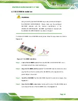
Page 55: ...se follow the steps below and refer to Figure 4 1 Figure 4 1 SO DIMM Installation Step 1 Locate the SO DIMM socket Place the WAFER CV D25501 N26001 on an anti static pad with the solder side facing up...

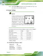
Page 56: ...E SHORT a jumper means connecting the pins of the jumper with the plastic clip and to OPEN a jumper means removing the plastic clip from a jumper The hardware jumpers must be set before installation J...

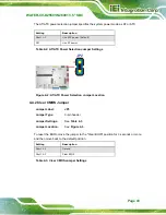
Page 57: ...on Jumper Settings Figure 4 2 AT ATX Power Selection Jumper Location 4 4 2 Clear CMOS Jumper Jumper Label JP3 Jumper Type 3 pin header Jumper Settings See Table 4 3 Jumper Location See Figure 4 3 To r...

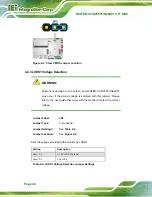
Page 58: ...voltage is selected with this jumper Please refer to the user guide that came with the monitor to select the correct voltage Jumper Label JP4 Jumper Type 3 pin header Jumper Settings See Table 4 4 Ju...

Page 59: ...ng voltage is selected with this jumper Please refer to the user guide that came with the monitor to select the correct voltage Jumper Label JP1 Jumper Type 3 pin header Jumper Settings See Table 4 5...

Page 60: ...channel Pin No 4321 EDID Resolution Color Depth Channel 0000 800 x 600 60 Hz 18 bit Single 0001 1024 x 768 60Hz 18 bit Single 0010 1024 x 768 60Hz 24 bit Single 0011 1280 x 768 60Hz 18 bit Single 010...

Page 61: ...24 bit Dual 1111 1920 x 1200 60Hz 24 bit Dual Table 4 6 LVDS2 Panel Resolution Figure 4 6 LVDS2 Panel Type Selection Switch Location 4 5 Chassis Installation 4 5 1 Heat Sink Enclosure WARNING Never r...

Page 62: ...astic desk It is highly recommended to run the WAFER CV D25501 N26001 on a heat dissipation surface or using copper pillars to hold the board up from the desk below When the WAFER CV D25501 N26001 is...

Page 63: ...N26001 to be mounted into a chassis please refer to Figure 1 3 for the detailed dimensions The user can design or select a chassis that has screw holes matching up with the holes on the heat sink enc...

Page 64: ...audio kit consists of three audio jacks One audio jack Mic In connects to a microphone The remaining two audio jacks Line In and Line Out connect to two speakers To install the audio kit please refer...

Page 65: ...CV D25501 N26001 please follow the steps below Step 1 Locate the connector The locations of the LVDS connectors are shown in Chapter 3 Step 2 Insert the cable connector Insert the connector from the...

Page 66: ...ight inverter connector The locations of the backlight inverter connectors are shown in Chapter 3 Step 4 Connect backlight connector Connect the backlight connector to the driver TFT LCD PCB as shown...

Page 67: ...Installation To install a full size PCIe Mini card please follow the steps below Step 1 Locate the full size PCIe Mini card slot The location of the full size PCIe Mini card slot is shown in Chapter 3...

Page 68: ...e Line up the notch on the card with the notch on the connector Slide the PCIe Mini card into the socket at an angle of about 20 Figure 4 13 Figure 4 13 Insert the Full size PCIe Mini Card into the So...

Page 69: ...CIe Mini card please follow the steps below Step 1 Locate the half size PCIe Mini card slot The location of the half size PCIe Mini card slot is shown in Chapter 3 Step 2 Remove the retention screws R...

Page 70: ...ure 4 16 Insert the Half size PCIe Mini Card into the Socket at an Angle Step 4 Secure the half size PCIe Mini card Secure the half size PCIe Mini card with the two retention screws previously removed...

Page 71: ...le Connection Step 3 Connect the cable to the SATA disk Connect the connector on the other end of the cable to the connector at the back of the SATA drive See Figure 4 18 Step 4 To remove the SATA cab...

Page 72: ...etention screws that must be secured to a chassis or bracket Step 4 Connect the serial device Once the single RS 232 connector is connected to a chassis or bracket a serial communications device can b...

Page 73: ...tor on the WAFER CV D25501 N26001 connect the cable connector to the on board connector See Figure 4 20 Figure 4 20 Keyboard mouse Y cable Connection Step 4 Attach PS 2 connectors to the chassis The k...

Page 74: ...WAFER CV D25501 N26001 3 5 SBC Page 60 both marked Please make sure the keyboard and mouse are connected to the correct PS 2 connector...

Page 75: ...WAFER CV D25501 N26001 3 5 SBC Page 61 Chapter 5 5 BIOS...

Page 76: ...soon as the system is turned on or 2 Press the DEL or F2 key when the Press DEL or F2 to enter SETUP message appears on the screen If the message disappears before the DEL or F2 key is pressed restart...

Page 77: ...ctions for the highlighted item appears To exit the Help Window press ESC or the F1 key again 5 1 4 Unable to Reboot after Configuration Changes If the computer cannot boot after changes to the system...

Page 78: ...Use Tab to switch between Data elements Select Screen Select Item Enter Select Change Opt F1 General Help F2 Previous Values F3 Optimized Defaults F4 Save Exit ESC Exit Version 2 14 1219 Copyright C...

Page 79: ...o Setup Utility Copyright C 2011 American Megatrends Inc Main Advanced Chipset Boot Security Save Exit ACPI Settings RTC Wake Settings CPU Configuration IDE Configuration USB Configuration F81866 Supe...

Page 80: ...Megatrends Inc BIOS Menu 3 ACPI Settings ACPI Sleep State S1 CPU Stop Clock Use the ACPI Sleep State option to specify the sleep state the system enters when it is not being used S1 CPU Stop Clock DEF...

Page 81: ...erican Megatrends Inc BIOS Menu 4 RTC Wake Settings Wake system with Fixed Time Disabled Use the Wake system with Fixed Time option to enable or disable the system wake on alarm event Disabled DEFAULT...

Page 82: ...r Hyper Threading Technology Select Screen Select Item Enter Select Change Opt F1 General Help F2 Previous Values F3 Optimized Defaults F4 Save Exit ESC Exit Version 2 14 1219 Copyright C 2011 America...

Page 83: ...the system Aptio Setup Utility Copyright C 2011 American Megatrends Inc Advanced SATA1 Not Present SATA2 Not Present Configure SATA as IDE Select a configuration for SATA Controller Select Screen Sele...

Page 84: ...F2 Previous Values F3 Optimized Defaults F4 Save Exit ESC Exit Version 2 14 1219 Copyright C 2011 American Megatrends Inc BIOS Menu 7 USB Configuration Legacy USB Support Enabled Use the Legacy USB Su...

Page 85: ...ral Help F2 Previous Values F3 Optimized Defaults F4 Save Exit ESC Exit Version 2 14 1219 Copyright C 2011 American Megatrends Inc BIOS Menu 8 Super IO Configuration 5 3 6 1 Serial Port n Configuratio...

Page 86: ...ted IO 3F8h IRQ 4 Serial Port I O port address is 3F8h and the interrupt address is IRQ4 IO 3F8h IRQ 3 4 Serial Port I O port address is 3F8h and the interrupt address is IRQ3 4 IO 2F8h IRQ 3 4 Serial...

Page 87: ...ort I O port address is 2F8h and the interrupt address is IRQ3 4 IO 3E8h IRQ 3 4 Serial Port I O port address is 3E8h and the interrupt address is IRQ3 4 IO 2E8h IRQ 3 4 Serial Port I O port address i...

Page 88: ...s IRQ10 11 IO 250h IRQ 10 11 Serial Port I O port address is 250h and the interrupt address is IRQ10 11 IO 2E0h IRQ 10 11 Serial Port I O port address is 2E0h and the interrupt address is IRQ10 11 5 3...

Page 89: ...e interrupt address is IRQ10 11 5 3 7 F81866 H W Monitor The F81866 H W Monitor menu BIOS Menu 10 contains the fan configuration submenus and displays operating temperature fan speeds and system volta...

Page 90: ...onitored are System Temperatures o CPU Temperature o System Temperature Fan Speeds o CPU Fan Speed o System Fan Speed Voltages o VCC_CPU o VCC_GFX o V1 05S o 1 5_DDR3 o VSB5V o V3 3S o VSB3V o VBAT 5...

Page 91: ...11 American Megatrends Inc BIOS Menu 11 Smart Fan Mode Configuration CPU_FAN1 SYS_FAN Smart Fan Control Auto Duty Cycle Mode Use the CPU_FAN1 or SYS_FAN1 Smart Fan Control option to configure the CPU...

Page 92: ...trends Inc BIOS Menu 12 Serial Port Console Redirection Console Redirection Disabled Use Console Redirection option to enable or disable the console redirection function Disabled DEFAULT Disabled the...

Page 93: ...one Use the Parity option to specify the parity bit that can be sent with the data bits for detecting the transmission errors None DEFAULT No parity bit is sent with the data bits Even The parity bit...

Page 94: ...stem automatically within 10 min when OS crashes Please install Auto Recovery API service before enabling this function Select Screen Select Item Enter Select Change Opt F1 General Help F2 Previous Va...

Page 95: ...ight C 2011 American Megatrends Inc Main Advanced Chipset Boot Security Save Exit Host Bridge South Bridge Host Bridge Parameters Select Screen Select Item Enter Select Change Opt F1 General Help F2 P...

Page 96: ...Intel IGD Configuration Use the Intel IGD Configuration submenu BIOS Menu 16 to configure the video device connected to the system Aptio Setup Utility Copyright C 2011 American Megatrends Inc Advance...

Page 97: ...system Configuration options are listed below 640x480 LVDS 800x600 LVDS DEFAULT 1024x768 LVDS 1280x1024 LVDS 1366x768 LVDS 1224x600 LVDS 1280x800 LVDS Backlight Control Inverted Use the Backlight Cont...

Page 98: ...ave Exit ESC Exit Version 2 14 1219 Copyright C 2011 American Megatrends Inc BIOS Menu 17 Southbridge Chipset Configuration Power Saving Function ERP Disabled Use the Power Saving Function ERP option...

Page 99: ...Version 2 14 1219 Copyright C 2011 American Megatrends Inc BIOS Menu 18 Boot Bootup NumLock State On Use the Bootup NumLock State BIOS option to specify if the number lock setting must be modified dur...

Page 100: ...sable boot option for legacy network devices Disabled DEFAULT Ignore all PXE Option ROMs Enabled Load PXE Option ROMs Option ROM Messages Force BIOS Use the Option ROM Messages option to set the Optio...

Page 101: ...er Setup In Setup the User will have Administrator rights The password must be 3 to 20 characters long Administrator Password User Password Set Setup Administrator Password Select Screen Select Item E...

Page 102: ...S Menu 20 Exit Save Changes and Reset Use the Save Changes and Reset option to save the changes made to the BIOS options and reset the system Discard Changes and Reset Use the Discard Changes and Rese...

Page 103: ...WAFER CV D25501 N26001 3 5 SBC Page 89 6 Software Drivers Chapter 6...

Page 104: ...be installed on the system Chipset Graphics LAN Audio Installation instructions are given below 6 2 Starting the Driver Program To access the driver installation programs please do the following Step...

Page 105: ...1 Chipset Step 3 Go to the 32 bit or 64 bit folder that corresponds to your OS version Step 4 Open the Intel Chipset Software Installation Utility folder Step 5 Double click the infinst_autol icon Ste...

Page 106: ...01 N26001 3 5 SBC Page 92 Figure 6 2 Chipset Driver Welcome Screen Step 8 Click Next to continue Step 9 The license agreement in Figure 6 3 appears Step 10 Read the License Agreement Step 11 Click Yes...

Page 107: ...WAFER CV D25501 N26001 3 5 SBC Page 93 Figure 6 3 Chipset Driver License Agreement Step 12 The Read Me file in Figure 6 4 appears Step 13 Click Next to continue Figure 6 4 Chipset Driver Read Me File...

Page 108: ...formed as shown in Figure 6 5 Figure 6 5 Chipset Driver Setup Operations Step 15 Once the Setup Operations are complete click Next to continue Step 16 The Finish screen appears Step 17 Select Yes I wa...

Page 109: ...ed desktop or not have signal to it after restarting from the graphics driver installation To work out this limitation press the Ctrl Alt F1 hotkey to switch the primary display to CRT mode To install...

Page 110: ...96 Step 5 The Welcome Screen in Figure 6 7 appears Figure 6 7 Graphics Driver Welcome Screen Step 6 Click Next to continue Step 7 The license agreement in Figure 6 8 appears Step 8 Read the License Ag...

Page 111: ...age 97 Figure 6 8 Graphics Driver License Agreement Step 10 The Read Me file in Figure 6 9 appears Step 11 Click Next to continue Figure 6 9 Graphics Driver Read Me File Step 12 Setup Operations are p...

Page 112: ...perations Step 13 Once the Setup Operations are complete click the Next icon to continue Step 14 The Finish screen appears Step 15 Select Yes I want to restart the computer now and click the Finish ic...

Page 113: ...Section 6 2 Step 2 Click 3 LAN Step 3 Go to the Win7 Install_Win7_7048_09162011 folder Step 4 Double click the setup icon Step 5 The Welcome screen in Figure 6 12 appears Figure 6 12 LAN Driver Welcom...

Page 114: ...100 Figure 6 13 LAN Driver Installation Step 9 The program begins to install Step 10 When the driver installation is complete the screen in Figure 6 14 appears Step 11 Click Finish to exit Figure 6 1...

Page 115: ...owing Step 1 Access the driver list See Section 6 2 Step 2 Click 4 Audio Step 3 Open the Win7 folder Step 4 Double click the Vista_Win7_R263 icon Step 5 The installation files are extracted as shown i...

Page 116: ...Step 7 Click Next to continue Step 8 The program begins to install Step 9 The installation progress can be monitored in the progress bar shown in Figure 6 17 Figure 6 17 Audio Driver Installation Ste...

Page 117: ...WAFER CV D25501 N26001 3 5 SBC Page 103 Figure 6 18 Audio Driver Installation Complete Step 11 Select Yes I want to restart my computer now and click Finish Step 12 The system reboots...

Page 118: ...WAFER CV D25501 N26001 3 5 SBC Page 104 Appendix A A Regulatory Compliance...

Page 119: ...interference that may cause undesired operation This equipment has been tested and found to comply with the limits for a Class A digital device pursuant to part 15 of the FCC Rules These limits are de...

Page 120: ...WAFER CV D25501 N26001 3 5 SBC Page 106 Appendix B B BIOS Options...

Page 121: ...Settings Auto 73 Serial Port Enabled 73 Change Settings Auto 73 Serial Port Enabled 74 Change Settings Auto 74 PC Health Status 76 CPU_FAN1 SYS_FAN Smart Fan Control Auto Duty Cycle Mode 77 CPU System...

Page 122: ...d 86 Launch PXE OpROM Disabled 86 Option ROM Messages Force BIOS 86 UEFI Boot Disabled 86 Administrator Password 87 User Password 87 Save Changes and Reset 88 Discard Changes and Reset 88 Restore Defa...

Page 123: ...WAFER CV D25501 N26001 3 5 SBC Page 109 Appendix C C Terminology...

Page 124: ...low amplitude signal represents a binary 0 while a high amplitude signal represents a binary 1 BIOS The Basic Input Output System BIOS is firmware that is first run when the computer is turned on and...

Page 125: ...cation software changes the bus to core frequency ratio and the processor core voltage FSB The Front Side Bus FSB is the bi directional communication channel between the processor and the Northbridge...

Page 126: ...bus has transfer speeds up to 1 5 Gbps and the SATA II bus has data transfer speeds of up to 3 0 Gbps S M A R T Self Monitoring Analysis and Reporting Technology S M A R T refers to automatic status c...

Page 127: ...WAFER CV D25501 N26001 3 5 SBC Page 113 Appendix D D Digital I O Interface...

Page 128: ...nerally control signals that control the on off circuit of external devices or TTL devices Data can be read or written to the selected address to enable the DIO functions NOTE For further information...

Page 129: ...etting the digital port as input INT 15H AL low byte value AH 6FH Sub function AL 9 Set the digital port as OUTPUT BL Digital I O input value D 3 Assembly Language Sample 2 MOV AX 6F09H setting the di...

Page 130: ...WAFER CV D25501 N26001 3 5 SBC Page 116 Appendix E E Watchdog Timer...

Page 131: ...l INT 15H is used to control the Watchdog Timer INT 15H AH 6FH Sub function AL 2 Sets the Watchdog Timer s period BL Time out value Its unit second is dependent on the item Watchdog Timer unit select...

Page 132: ...the system resets EXAMPLE PROGRAM INITIAL TIMER PERIOD COUNTER W_LOOP MOV AX 6F02H setting the time out value MOV BL 30 time out value is 48 seconds INT 15H ADD THE APPLICATION PROGRAM HERE CMP EXIT_A...

Page 133: ...WAFER CV D25501 N26001 3 5 SBC Page 119 Appendix F F Hazardous Materials Disclosure...

Page 134: ...s and lamps These components will be separately marked Please refer to below table Toxic or Hazardous Substances and Elements Part Name Lead Pb Mercury Hg Cadmium Cd Hexavalent Chromium CR VI Polybrom...

Page 135: ...6001 3 5 SBC Page 121 RoHS RoHS Pb Hg Cd CR VI PBB PBDE O O O O O O O O O O O O O O O O O O O O O O O O O O O O O O O O O O O O O O O O O O O O O O O O O SJ T11363 2006 GB T 26572 2011 X SJ T11363 200...

Reviews: