


2. Signal Descriptions > PCIe Interface Signals
14
PEB383 User Manual
July 25, 2011
Integrated Device Technology, Inc.
Confidential - NDA Required
2.2
PCIe Interface Signals
PCIE Diff Out
PCIe differential output
PCIE Diff In
PCIe differential input
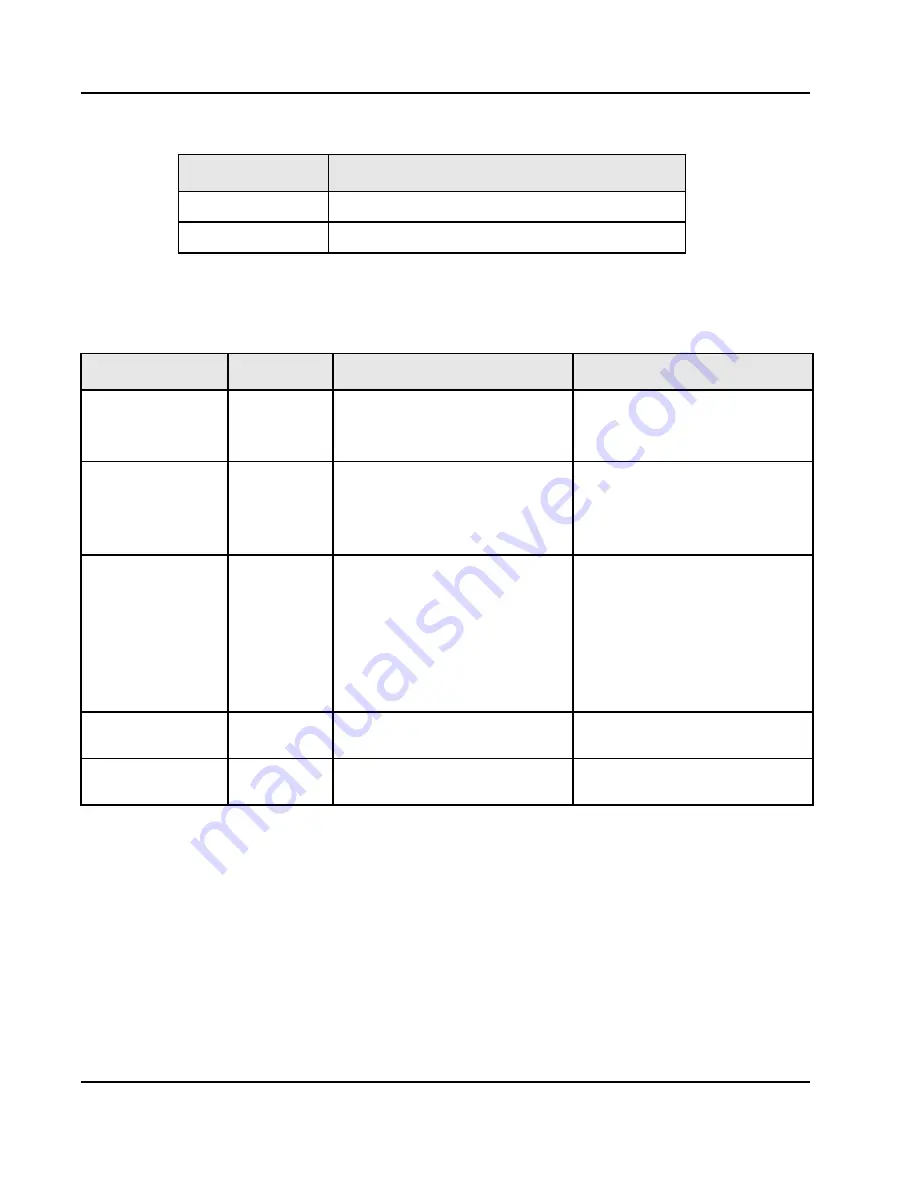
Table 2: PCIe Interface Signals
Name
Pin Type
Description
Design Recommendation
PCIE_PERSTn
3.3 In
Master reset in:
0 = PEB383 in reset
1 = PEB383 in normal mode
Direct connect to the PERST# signal.
PCIE_TXD_n
PCIE_TXD_p
PCIE Diff Out
Transmit Data. These differential pair
signals send PCIe 8b/10b encoded
symbols and an embedded clock to the
link partner.
DC blocking capacitors must be placed
in the link between the transmitter and
the receiver. Place a 0603 or 0402
0.075uF to 0.1uF ceramic capacitor on
each TXD_n, TXD_p signal.
PCIE_RXD_n
PCIE_RXD_p
PCIE Diff In
Receive Data. These differential pair
signals receive PCIe 8b/10b encoded
symbols and an embedded clock from
the link partner.
DC blocking capacitors must be placed
in the link between the transmitter and
the receiver; however, the DC blocking
capacitors are normally placed near the
transmitter. When designing an add-in
card, capacitors are not required on this
link. When designing a system board,
the DC blocking capacitors should be
placed near the transmitter.
PCIE_REFCLK_n
PCIE_REFCLK_p
PCIE Diff In
Reference Clock. 100-MHz differential
reference clock.
Refer to Board Design Guidelines.
PCIE_REXT
Analog
-
This signal must be connected to VSS
with a 191-ohm (1%) resistor.
Table 1: Pin Types
(Continued)
Pin Type
Definition


