background image

TC- 446 Service Manual

8

Circuit Description

1.

Frequency Configuration

The receiver utilizes double conversion superheterodyne. The first IF is 21.4MHz and the second

is 455KHz. The first local oscillator signal is supplied from PLL circuit. Frequency needed in the

transmitter is supplied from PLL circuit. Figure 1 shows the frequency configuration.

Frequency Range:

446.00625 MHz— 446.09375MHz

Figure 1 frequency configuration

2.

Receiver

The receiver utilizes double conversion superheterodyne.

1) Front-end RF Amplifier

The input signal from antenna is amplified in RF amplifier (Q27) after passing through

the receive/transmit switch circuit and a 3-stage LC band pass f ilter. The amplified

signals are filtered by a band pass filter (a 3-stage LC BPF) to eliminate unwanted

signals before they goes to the first frequency mixer.

Figure 2 receiver section configuration

Summary of Contents for TC-446

Page 1: ...www hyt com cn ...

Page 2: ......

Page 3: ...scription 4 Circuit Description 8 CPU Pins 12 Part List 1 14 Adjustment Description 26 Troubleshooting chart 29 Disassembly and Assembly 42 Exploded View 45 Part List 2 46 Packing 48 PC Board View 49 Block Diagram 50 Schematic Diagram 51 Specifications 52 ...

Page 4: ...aps or in an explosive atmosphere When in vehicles with an airbag do not place a portable radio in the area over an airbag or in the airbag deployment area Do not expose the radio to direct sunlight for a long time nor place it close to a heating source Do not use any portable radio with a damaged antenna If a damaged antenna comes into contact with your skin a minor burn may result When transmitt...

Page 5: ...to turn the radio on fully counter clockwise until a click is heard to turn the radio off When the radio is on turn the knob to adjust volume 5 PTT key Press and hold PTT key to talk release to receive 6 Monitor key In receive mode long press above 2 seconds Monitor key to monitor activity on the current channel 7 Microphone 8 Speaker 9 External jack Remove the jack cover and insert an earphone or...

Page 6: ...dard model please disconnect the two MS2 points on PCB and then operate the following steps 2 To select MS1 See the initial data table according to the radio model if MS1 is 1 short out the two MS1 points on PCB and continue the following operation If not disconnect the two MS1 points and continue 3 Short out the two SELF points on PCB and then turn the power on Two beeps sound 4 Turn channel sele...

Page 7: ...he following parameters can be set via PC programming software 1 Low battery alert level 2 Squelch level 9 3 Squelch level 3 4 CTCSS deviation narrow 5 CDCSS deviation narrow 5 Manual Adjust Mode If manual adjust mode is enabled turn on the power while holding down PTT and MONI simultaneously the radio enters manual adjust mode after 2 seconds Choose the adjusting items by turning the channel sele...

Page 8: ... MONI again to begin user wired clone and red LED blinks When cloning is completed red LED goes out 2 If the two SELF points are short circuit press MONI again to begin factory wired clone and red LED blinks When cloning is completed red LED goes out Note The difference between user wired clone mode and factory wired clone mode is that the latter is able to clone tune parameters ...

Page 9: ... Frequency MHz IF MHz 1CH 2CH 3CH 4CH 5CH 6CH 7CH 8CH 9 16CH Tx MHz Rx MHz Tx MHz Rx MHz Tx MHz Rx MHz MHz MHz MHz MHz MHz MHz Standard 446 00625 446 09375 21 4 446 00625 446 00625 446 05625 446 05625 446 03125 446 03125 446 08125 446 01875 446 06875 446 04375 446 09375 CH QT DQT OFF OFF OFF OFF 97 4 97 4 71 9 79 7 67 85 4 023 ...

Page 10: ...ncy configuration Frequency Range 446 00625 MHz 446 09375MHz Figure 1 frequency configuration 2 Receiver The receiver utilizes double conversion superheterodyne 1 Front end RF Amplifier The input signal from antenna is amplified in RF amplifier Q27 after passing through the receive transmit switch circuit and a 3 stage LC band pass filter The amplified signals are filtered by a band pass filter a ...

Page 11: ...C7 1 4 and then filtered by low pass filter Q19 and high pass filter Q20 and then de emphasized by R130 and C156 The resulting AF signal passes through a volume control circuit and then is amplified to a sufficient level to drive the speaker by AF power amplifier IC8 5 Squelch Part of the AF signal from IC1 enters IC1 again and the noise component is amplified and rectified by a filter and an ampl...

Page 12: ... oscillator VCO passes through buffer amplifier Q14 and is divided at IC2 by the dual module programmable counter The divided signal is compared in the phase comparator IC2 with the 2 5 KHz or 6 25 KHz reference signal The output signal from phase comparator is filtered through a low pass filter and passed to the VCO to control the oscillator frequency See figure 4 Figure 4 PLL circuit 2 VCO The o...

Page 13: ...plifier The transmit signal obtained from VCO buffer amplifier Q14 is amplified by Q15 and Q17 This amplified signal is passed to power amplifier Q32 and Q31 and is capable of producing a 4 0W RF power 4 Antenna Switch and LPF The RF amplifier output signal is passed through a low pass filter network and a transmit receive switch circuit before it is passed to the antenna terminal The transmit rec...

Page 14: ...ute control H Mic mute L Mic enable 16 MS1 I Model set 17 GREEN O Green light control H light 18 RED O Red light control H light 19 TXD O RS 232C output 20 RXD I RS 233C input 21 PTTK I PTT key input 22 MS2 I Standard model select H Non standard L Standard 23 RXC O Receiver power control L power on 24 NC 25 RESET I Reset input 26 SELF I Self program L on 27 TXC O Transmitter power control H on 28 ...

Page 15: ...TCSS code output 42 TONE4 O CTCSS code output 43 TONE3 O CTCSS code output 44 TONE2 O CTCSS code output 45 TONE1 O CTCSS code output 46 TONE0 O CTCSS code output 47 WNTC O W N L Wide H Narrow 47 70 NC 71 Vcc I Power input 5V 72 VREF I A D converse reference voltage 73 Avss I A D GND 74 77 NC 78 NC 79 NC 80 NC ...

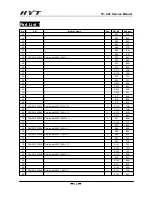
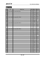
Page 16: ...5 R508 B5B 16 R601 B1E 17 R602 B3C 18 3001061000000 Chip resistor 0603 10Ω J 1 10 6 R112 T3E 19 R113 T5J 20 R164 B2C 21 R196 B4G 22 R80 B2D 23 R82 B4G 24 3001061010000 Chip resistor 0603 100Ω J 1 1 6 R127 B5F 25 R147 B4E 26 R74 B2C 27 R75 B4J 28 R76 B5E 29 R90 T5H 30 3001061020010 Chip resistor 0603 1KΩ J 1 10 12 R203 T2E 31 R39 B3B 32 R51 B1F 33 R52 T3F 34 R53 B2D 35 R56 B2B 36 R57 B5B 37 R58 T4B...

Page 17: ...istor 0603 1MΩ J 1 10 2 R109 T2B 68 R116 T3B 69 3001061230000 Chip resistor 0603 12KΩ J 1 1 2 R170 B1D 70 R617 B4H 71 3001061240010 Chip resistor 0603 120KΩ J 1 3 R11 B3B 72 R124 T3F 73 R72 B2D 74 3001061510000 Chip resistor 0603 150Ω J 1 1 2 R68 B2E 75 R69 B2C 76 3001061520000 Chip resistor 0603 1 5KΩ J 1 3 R48 B3E 77 R50 T5F 78 R55 T2E 79 3001061530010 Chip resistor 0603 15KΩ J 1 1 3 R161 T4F 80...

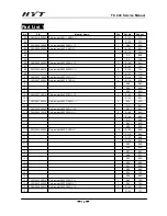
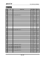
Page 18: ...B 102 R49 B4D 103 R64 B2G 104 R65 B2G 105 3001062730010 Chip resistor 0603 27KΩ J 1 1 2 R102 B3H 106 R132 B3C 107 3001062740010 Chip resistor 0603 270KΩ J 1 2 R16 B3D 108 R2 B3C 109 3001063020000 Chip resistor 0603 3KΩ J 1 10 1 R81 B3F 110 3001063310010 Chip resistor 0603 330Ω J 1 1 5 R122 B3G 111 R146 B4D 112 R5 B4E 113 R67 B2D 114 R96 B2B 115 3001063320000 Chip resistor 0603 3 3KΩ J 1 14 R135 B4...

Page 19: ...05 B1E 153 R128 B3B 154 R4 T2B 155 R54 T3G 156 R606 T3I 157 R607 T3I 158 R608 T3I 159 R609 T3I 160 R610 T2C 161 R615 B3B 162 R93 T2F 163 3001064740010 Chip resistor 0603 470KΩ J 1 2 R22 T1D 164 R94 T3F 165 3001065620010 Chip resistor 0603 5 6KΩ J 1 2 R130 B4B 166 R79 B2D 167 3001065630000 Chip resistor 0603 56KΩ J 1 1 4 R149 B3E 168 R157 T4F 169 R198 T4E 170 R627 171 3001065640000 Chip resistor 06...

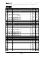
Page 20: ...T1B 194 VR5 195 3005991030070 Array resistor 0603 10KΩ 4 J 1 2 CP1 T1B 196 CP6 T4A 197 3005061030040 Array resistor 0603 10KΩ 2 J 1 1 CP5 T1B 198 3005064720000 Array resistor 0603 4 7KΩ 2 J 1 1 CP4 T1B 199 3005064720010 Array resistor 0603 4 7KΩ 4 J 1 1 CP3 T1B 200 3101050100000 Chip capacitor 0402 1PF C 50V 4 C104 B4G 201 C143 B4I 202 C146 B4I 203 C95 B1E 204 3101050200010 Chip capacitor 0402 2PF...

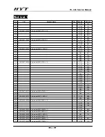
Page 21: ...1 C253 232 C255 233 C88 B2E 234 3101051010030 Chip capacitor 0402 100PF J 50 6 C132 B2D 235 C15 B2A 236 C16 B2A 237 C17 B2A 238 C179 B3C 239 C180 B2A 240 3101051020010 Chip capacitor 0402 1000PF K 5 30 C109 B2C 241 C110 B2C 242 C111 B4H 243 C113 B2B 244 C114 B3H 245 C121 B2E 246 C147 B4I 247 C252 248 C26 B2B 249 C59 B1G 250 C60 B1G 251 C61 B2G 252 C62 B2G 253 C65 B1C 254 C66 T1E 255 C68 B3H 256 C6...

Page 22: ...1051040040 Chip capacitor 0402 0 1UF K 10 15 C178 T2B 286 C233 B4E 287 C246 B3B 288 C250 T3E 289 C37 B4B 290 C38 B4C 291 C39 B4D 292 C40 T2F 293 C43 B3C 294 C45 B5B 295 C46 B3C 296 C50 T4G 297 C51 B3I 298 C64 T2F 299 C84 T2E 300 3101051590000 Chip capacitor 0402 1 5PF B 50 2 C140 B4I 301 C196 B3E 302 3101051810000 Chip capacitor 0402 180PF J 50 1 C18 B5B 303 3101051830000 Chip capacitor 0402 0 018...

Page 23: ...B 322 C53 B4B 323 C54 B4C 324 3101053320010 Chip capacitor 0402 3300PF K 5 1 C166 T5F 325 3101053330000 Chip capacitor 0402 0 033UF K 5 C150 B4B 326 C151 B4B 327 C152 B4B 328 C153 B4B 329 C160 B3D 330 3101053340000 Chip capacitor 0402 0 33UF K 6 2 C126 B1B 331 C133 B4G 332 3101053900000 Chip capacitor 0402 39PF J 50V 1 C138 B3H 333 3101053920000 Chip capacitor 0402 3900PF K 2 1 C181 T2C 334 310105...

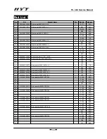
Page 24: ... Chip capacitor 0603 1PF B 50V 1 C92 B2C 371 3101060200010 Chip capacitor 0603 2PF B 50V 1 C93 B4E 372 3101060600010 Chip capacitor 0603 6PF B 50V 1 C145 B4J 373 3101061020000 Chip capacitor 0603 1000PF K 5 4 C198 T4G 374 C235 B4J 375 C63 B1D 376 C72 B3D 377 3101061040010 Chip capacitor 0603 0 1UF K 16 4 C194 T4H 378 C48 T4G 379 C49 T4G 380 R200 B2B 381 3101061800000 Chip capacitor 0603 18PF J 50V...

Page 25: ...02 18nH LQG15 1 L26 B2B 414 3210305220000 Multi layer inductor 0402 22nH LQG15 3 L18 B2D 415 L19 B2D 416 L25 B3E 417 3212105101000 Multi layer inductor 0402 100nH HK10 4 L17 B1C 418 L40 B5E 419 L47 B2C 420 L48 B1C 421 3212105470000 Multi layer inductor 0402 47nH HK100 2 L39 B5E 422 L45 B2D 423 3212106339000 Multi layer inductor 0603 3 3nH HK16 1 L29 B3H 424 3213212102000 Multi layer inductor 1008 ...

Page 26: ... 3307110100080 LED KPT 1608SGC ultra high 1 D22 T3J 464 3307110100070 LED KPT 1608SRC ultra high 1 D24 T3J 465 3399990000160 Varactor MA2Z36000L 30V 1 D4 B1D 466 3399990000220 Diode UDZ3 0B SOD 323 1 D10 B2B 467 3401001000080 Transistor 2SA1362 ER TE85 1 Q40 T3F 468 3401002000990 Transistor 2SC5108 Y TE85L 3 Q13 B2B 469 Q14 B2D 470 Q22 B4D 471 3403007000000 Transistor DTA114EE TL PNP 1 Q10 B4D 472...

Page 27: ...13 P 1 Q32 B3G 503 3504990000020 FET RD07MVS1 T112 P 1 Q31 B3I 504 3602028004610 AF amplification IC KIA6278F EL P 1 IC8 T3E 505 3603002005440 IF processing IC TA31136FNG EL 1 IC1 B4C 506 3603008005040 Operational amplifier NJM2902V 4 OA J 1 IC7 B3C 507 3604002055090 PLL TB31202FN EL ELP 1 IC2 B2A 508 3605008005010 Operational amplifier NJM2100V 2 OA J 1 IC3 T4F 509 3608015000000 Power managing IC...

Page 28: ...or details 2 Adjustment Some items can be adjusted in conventional communication mode and the others in manual adjust mode Turn on the power the radio enters conventional communication mode If manual adjust mode is enabled turn on the power while holding down PTT and MONI simultaneously the radio enters manual adjust mode after 2 seconds Refer to the section Software Specification VCO Item Conditi...

Page 29: ...tch N W Radio Communicati on Test Set 118dBm MOD 1KHz 1 5kHz Narrow FILER 0 3 3 4kHz ANT Speaker Jack Check SINAD 12dB or higher 2 RX Low Turn to CH14 in manual adjust mode long press MONI key to switch N W 3 RX High Turn to CH15 in manual adjust mode long press MONI key to switch N W 6 Squelch 1 RX Center Turn to CH2 in manual adjust mode Adjust by pressing PTT or MONI Radio Communic ation Test S...

Page 30: ... on condition 1 and condition 2 are consistent the difference 200Hz 67 0Hz CTCSS 2 CTCSS 250 3Hz Turn to CH16 in manual adjust mode and press PTT 250 3Hz CTCSS 11 CTCSS Deviation 1 TX Center Turn to CH4 wide and CH4 narrow in manual adjust mode Adjust by pressing PTT or MONI Radio Communication Test Set HPF 20Hz LPF 300Hz ANT Adjust deviation to 0 4kHz 100Hz Narrow 12 CDCSS Deviation 1 Turn to CH5...

Page 31: ...ard from SPK Inject 21 4MHz signal into XF1 IN SSG output 103dbm Audio heard from SPK Check CF1 455K2nd IF filter IC1 IF IC X1 20 945M 2nd LO CD1 demodulator Check XF1 1 st IF filter Q22 Replace faulty components Inject 1KHz RX signal into Q27 RF AMP IN SSG 113dbm Audio heard from SPK Power supply at Q9 5R OK Check Q23 mixer Q27 Tc5 Replace faulty Check if no solder joint at IC11 pin 23 Check Q9 R...

Page 32: ... 2 Symptom TX OK low RX sensitivity or intermittent RX output Cure replace 455KHz filter 3 Symptom TX OK low RX sensitivity but sensitivity OK after injecting 45 05MHz signal into XF1 Cure adjust TC3 TC4 and TC5 in turn 2 No RX audio output no audio from SPK sound abnormal Symptom 1 no audio after power on no or low audio in monitor mode activate power on alert tone and monitor features ...

Page 33: ... AMP pin1 Check VR1 and its wiring to IC8 Replace faulty components Hold down MONI 6V voltage at IC8 pin8 Hold down MONI 5V output at IC11 pin40 AVP Audio output at IC8 pin 7 Check if Q39 and Q12 conductive Replace faulty components Check C203 c239 Replace faulty components See control section troubleshooting Check R203 R37 C84 C66 Check IC8 and peripheral components Replace faulty components Q41 ...

Page 34: ...NI 6 0V voltage at IC8 pin8 but no audio output at pin7 Cure replace IC8 Start Hold down MONI Audio output at IC7 pin1 Check if Q21 conductive Check operating status of Q19 Q20 Check C44 C150 C151 C152 C153 C45 Replace faulty components Hold down MONI Audio output at IC7 pin3 5V voltage at IC7 pin4 5V voltage at IC1 IF pin4 Check IC7 IC11 peripheral components Replace faulty components Check the c...

Page 35: ... but no or low power output in TX In TX 6 0V source voltage at Q31 In TX around 1 1W power at D11 positive end In TX 1 8 2 5 V gate voltage at Q31 Check Q32 Q17 Q38 peripheral components Replace faulty components In TX 7 5V source voltage and 1 8 2 5V gate voltage at Q32 Check C30 C139 C142 C141 C145 Replace faulty components Check D11 R75 C208 L4 Check bias circuit Replace Q31 Check L3 Q31 C55 In...

Page 36: ...eters and D5 positive bias OK Replace faulty components Check bias circuit 4V collector voltage 1 8V base voltage and 1V emitter voltage at Q15 Check R80 L18 R34 R29 R79 C97 arameters OK Replace with components of the same spec See VCO Troubleshootin R122 C98 R196 C42 R195 OK In TX 4 8V collector voltage 1 2V base voltage and 0 3V emitter voltage at Q17 L29 C138 C67 OK N Y Y Y N Y N Y N ...

Page 37: ...ect 1KHz 100mv AF signal into MIC plug 4 2KHz 150Hz modulation deviation Check MIC plug and MIC Replace faulty components Waveform input at IC3 NJM2100V pin2 OK Check L14 C48 C169 C168 Replace faulty components In TX amplified waveform output at IC3 pin7 In TX 5V voltage at IC3 pin 8 In TX waveform output at VR2 Check IC3 and peripheral components Check the connection to Q4 C pin Check components ...

Page 38: ...epair Example 1 Symptom no TX audio cracked VR2 Cure replace VR2 and adjust 2 Symptom low TX audio poor modulation sensitivity of MIC after adjusting VR2 Cure replace MIC II PLL 1 TX or RX unlock Caused by faulty oscillator loop ...

Page 39: ...tput voltageat Q7 Reliable solder and correct parameters of R164 R9 L47 Q8 InRX 4 3Vat IC11pin31 Check IC11 peripheral components or replace IC11 Reliable solder at Q7 R53 No disconnected wiring to branch circuit 4Voutput voltageat Q6 Reliable solder at R171 No disconnected wiringto Q16 branch circuit In TX 0V at IC11pin31 Reliable solder at PTT No disconnected wiring to IC11branch circuit Or repl...

Page 40: ...joints at IC11 pin6 Correct software settings If not replace IC11 Check Q3 R65 Q2 R28 R66 Replace faulty components 12 8MHz at IC2 pin13 Check 12 8MHz crystal C130 TC6 Replace faulty components After amplified by Q13 VCO output OK Check VCO circuit Data clock strobe pulse at IC2 pin8 9 10 OK triangle wave Check CP6 CPU C15 C16 C17 and wiring 1 4V CV control voltage output Check the soldering and v...

Page 41: ...radio via PC no 5V output at Q5 Cure replace Q5 717 4 Symptom unable to transmit even if PTT is pressed freq range found OK when reading from radio via PC 5V output at Q5 5C voltage at X2 12 8 crystal oscillator Cure replace X1 5 Symptom able to transmit when PTT is pressed freq range found OK when reading from radio via PC 5C voltage OK Voltage found at CV in RX but not within 0 8 4V Cure adjust ...

Page 42: ...utput at L15 Upper Check L15 C149 C120 Replace faulty components Switch on power 6 0V at IC4 IN Check power switch D20 IC4 Replace faulty components 5V at IC4 OUT Check if short circuit occurs when IC4 C80 C79 branch circuit are grounded Replace faulty components Check IC11 pin 71 72 5V at IC9 pin 5 RESET Check if no solder at IC11 and branch components Replace faulty components Start Check IC11 X...

Page 43: ... 5V at IC4 IN power knob OK Cure replace D20 2 Symptom Plug in 6 0 power cable rotate power knob but unable to switch on power Voltages at L15 IC4 IN OK no 5V 5M voltage at IC4 Cure replace IC404 3 Symptom Plug in 6 0 power cable rotate power knob but unable to switch on power 5V output at IC4 Voltage at IC9 OK Cure replace X3 7 3728MHz crystal ...

Page 44: ...ay from the radio s body and lift the battery from the radio See figure 1 Figure 1 Disassemble main unit aluminum chassis and PCB 1 Remove the two screws at the base of the chassis 2 Pull the volume knob and selector knob off 3 Remove the antenna at top of the radio 4 Remove the screw of the microphone jack cover and pull the jack cover off See figure 2 Figure 2 ...

Page 45: ... upwards and then pull the chassis away from the front cover See figure 3 Figure 3 The disassembly is shown as the figure 4 Figure 4 Disassemble PTT button Push the PTT button in indicated direction until out of the cover See figure 5 Figure 5 ...

Page 46: ...n press the PTT button into the corresponding opening in the cover See figure 6 Figure 6 Attach the battery 1 Fit the extensions at the bottom of the battery into the slots on the radio chassis 2 Press the top part of the battery towards the radio until a click is heard See figure 7 Figure 7 ...

Page 47: ...TC 446 Service Manual 45 Exploded View 1 7 6 8 16 15 10 11 9 18 21 19 22 23 13 14 17 20 24 25 26 27 28 29 30 31 32 33 34 35 36 37 38 39 2 4 3 5 12 ...

Page 48: ...ponge 1 5mm thick EVA 1 10 6201030000000 TC 500 Battery positive electrode piece 0 20mm SUS301 nickel plating 1 11 6000046000000 TC2100 Positive electrode piece support Black ABS 1 12 7207002200000 Nut M7 0 2 2mm 1 13 4303020000030 Volume switch TC 1688 1 14 7206002500010 Nut M6 0 2 5mm 1 15 4302030000010 Channel switch TC 368 RY 6933 tocos 1 16 4301040000020 PTT switch TC 278 TC 378 SKHLLBA010 AL...

Page 49: ...jack HSJ1456 010320 1 33 5205000000190 Earpiece jack HSJ1650 010020 1 34 7400133000000 TC500 PVC water proof gasket PVC 0 3mm thick Φ4 7 2 35 7500115000000 TC500 Battery contact pad Silica rubber 4 8 4 2mm 2 36 6201022000000 TC2100 Battery negative electrode piece 0 20mm SUS301 nickel plating 1 37 7400014000010 TC 500 Battery water proof PVC piece 0 2mm thick PVC 18 40 16 10mm 1 38 6000039000000 T...

Page 50: ...TC 446 Service Manual 48 Packing ...

Page 51: ......

Page 52: ......

Page 53: ... 0 022U C169 0 022U C48 0 1U R131 1 8K R50 1 5K R160 750K R161 15K R162 15K R120 22K R110 0 C173 4 7U 16V C76 1000P C49 0 1U C77 1000P C50 0 1U D18 1SS372 C174 1U 16V D19 DAN222 ACTIVE FILTER ACTIVE FILTER Q26 2SC5343 s R163 15K L14 1uH R165 2 2K R166 470 C125 10u 10V C35 470p Mic MIC1 TC3 10P TC4 10P L38 3T J3 SPK 4Ω VR2 47K R58 1K R18 100K L41 0 22u R19 NC R20 NC R21 NC L42 NC X3 C175 33p C176 3...
Page 54: ...ation distortion 5 Modulation limiting 5KHz wide 2 5KHz narrow Bandwidth 16 KHz wide 8 5KHz narrow Audio response From 6 dB oct Pre Emphasis 3dB Conducted spurious emission 7 5μW Adjacent channel power 65 d B Receiver Reference sensitivity 0 25μV wide 0 35uV narrow Unsquelch sensitivity 0 4μV Audio power 400mW 4Ω Audio distortion 5 Modulation acceptance 7 KHz wide 3 5KHz narrow Audio response From...

Reviews: