background image

Electrical aspects for the companion solution

40/108

5.2

Block diagram for the companion solution

The following block diagram explains how to apply the netRAPID 90 within
the companion solution:

Figure 17: netRAPID - Companion solution

netRAPID 90 | Design guide
DOC190601DG01EN | Revision 1 (Draft 10) | English | 2019-09 | Preliminary | Public

© Hilscher 2019

Summary of Contents for netRAPID 90

Page 1: ...Design guide netRAPID 90 Chip Carrier Hilscher Gesellschaft f r Systemautomation mbH www hilscher com DOC190601DG01EN Revision 1 Draft 10 English 2019 09 Preliminary Public...

Page 2: ...view netRAPID 90 products 15 2 4 2 Memory options 15 2 4 3 Preloaded vs open platform 16 2 5 Solutions for typical applications 17 2 5 1 Companion solution providing a fixed layout 17 2 5 2 Stand alon...

Page 3: ...ard 55 7 1 Positions of elements Evaluation board NRPEB H90 RE 55 7 2 Operating elements of the evaluation Board 57 7 2 1 Switches and buttons 57 7 2 2 Jumper field X501 63 7 3 Interfaces 64 7 3 1 Fie...

Page 4: ...dules 87 8 2 1 RS232 interface module 88 9 Schematics 89 9 1 NRPEB H90 RE Front view 89 9 2 NRPEB H90 RE ETHERNET 90 9 3 NRPEB H90 RE FTDI 91 9 4 NRPEB H90 RE IO ADC 92 9 5 NRPEB H90 RE NETRAPID 93 9...

Page 5: ...is document refers to the following other documents Hilscher Gesellschaft f r Systemautomation mbH Getting Started Guide Serial Dual Port Memory Interface with netX Revision 4 English 2015 Hilscher Ge...

Page 6: ...panion solution Preloaded communication module You can use netRAPID 90 as companion solution in the style of a communication module to be connected with a host CPU In this scenario netRAPID 90 comes p...

Page 7: ...etX license and support agreement as well as the purchase of appropriate protocol stacks are required In this scenario the netRAPID 90 is provided as a pure hardware platform Note For more information...

Page 8: ...ices Using netX90 internal memory only Channel 0 Real Time Ethernet or Fieldbus Slave Channel 1 Network Services e g TCP socket or NDIS Basic WebServer Configuration via packets only Full featured fir...

Page 9: ...tion tasks to be executed on separated Cortex M4 processors Energy efficient SoC with lowest power loss 1 W Support for all Industrial Ethernet Fieldbus and IIoT standards providing a huge amount of f...

Page 10: ...he SSL TLS protocols and supports the following encryption algorithms Algorithm Supported key length RSA 4096 ECC 512 AES 256 SHA 512 Table 2 Supported encryption algorithms in netX 90 There is no TPM...

Page 11: ...erred via channel Channel 0 Real Time Ethernet data CIFX API Channel 1 TCP socket Raw Ethernet interface Channel 2 IIoT data netPROXY API Table 3 COM channels for cyclic and acyclic data to the applic...

Page 12: ...y to field and cloud Scalable platform for different use cases Preloaded and ready to use Energy efficient for extended temperature range 2 3 2 Requirements for design in Take the following items into...

Page 13: ...onnections of the netRAPID 90 chip carrier regardless of the mode they are intended for companion solution or stand alone solution Figure 3 Block diagram of NRP H90 RE and its interfaces netRAPID 90 D...

Page 14: ...t development risk EOL and part obsolescence handling by Hilscher RTE or FB interface in one design Reduced design and production costs PCB complexity and costs are encapsulated Baseboard can be done...

Page 15: ...CC Fieldbus interface module for CC Link 7923 740 Firmware for Real Time Ethernet Slave NXLFW ECS Loadable EtherCAT Slave Firmware 7428 120 NXLFW EIS Loadable EtherNet IP Adapter Firmware 7428 830 NX...

Page 16: ...B planned 56 pieces F8D8 1008 pieces F8D8 2520 pieces F8D8 NRP H90 RE PLS planned 56 pieces F8D8 1008 pieces F8D8 2520 pieces F8D8 NRP H90 RE CCIBS planned 56 pieces F8D8 1008 pieces F8D8 2520 pieces...

Page 17: ...been combined together within one single module The netX 90 within the netRAPID has two integrated ARM Cortex M4 cores in order to separate COM and APP Full access to both ARM Cortex M4 cores One des...

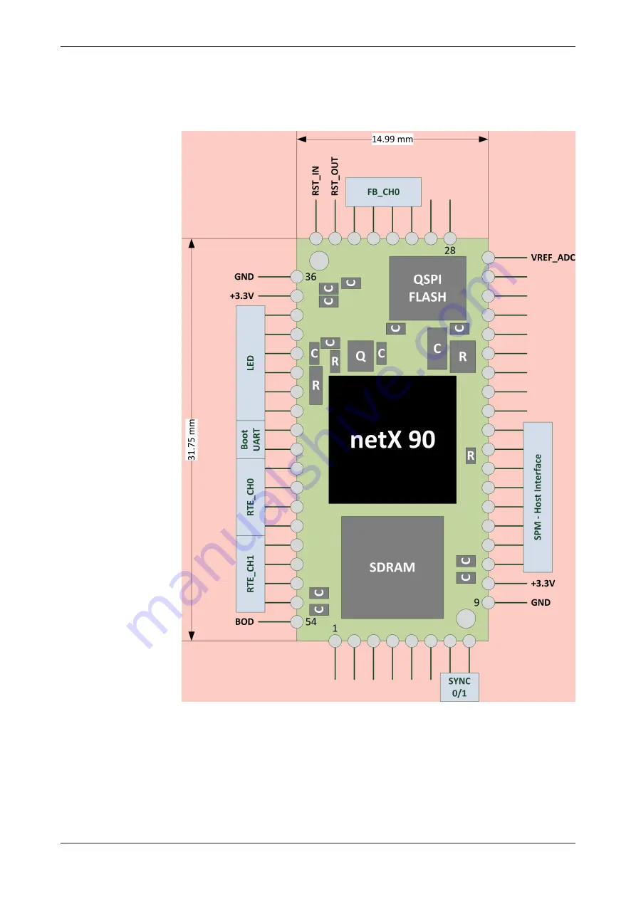
Page 18: ...D 90 chip carrier has the following dimensions Length 31 75 mm corresponding to 1250 mil Width 15 00 mm corresponding to 590 mil Height 4 mm netRAPID 90 Design guide DOC190601DG01EN Revision 1 Draft 1...

Page 19: ...1 30 29 28 1 3 048 mm 15 875 mm 1 27 mm 1 27 mm 3 062 mm 9 10 11 12 13 14 15 16 17 18 19 20 21 22 23 24 25 26 54 52 51 50 38 49 48 47 46 45 44 43 42 41 40 39 37 36 27 1 mm 1 524 mm 1 27 mm 3 048 mm Th...

Page 20: ...and trade a decrease of the MTBF of his devices for a higher temperature range specification netRAPID devices require a thermal pad at the bottom for heat dissipation to the PCB of the host system No...

Page 21: ...can be stored up to 1 year After 1 year the netRAPID devices have to be tempered again before soldered onto a host system Soldering netRAPID devices can be placed on the PCB of the host system for SM...

Page 22: ...s on the device for identification It contains 3 items 1 Part number 2 Hardware revision 3 Serial number The figure shows part number 7690 102 denoting NRP H90 RE F8D8 hardware revision 1 and serial n...

Page 23: ...signals GND_01 and GND_02 The SYS LED indicates the current system status of the module Note Power supply and ground should be connected at the shortest distance to the power and ground plane of the h...

Page 24: ...antly on the loaded firmware Note The reset signal RST_IN is not compatible to a voltage of 5 V Exceeding the voltage than 3 3 V DC by more than 5 may cause irreversible damage to the netRAPID 90 modu...

Page 25: ...pull up resistor Figure 8 Reset Logic OUT Recommendation Keep the signal way of RST_OUT_N short 4 2 3 Boot signal and boot options Boot modes The NRP H90 RE can be operated in the following three diff...

Page 26: ...uation board Console mode If the ROM code neither finds a valid firmware to start in standard boot mode nor a valid maintenance firmware to start in alternative boot mode it will start the console mod...

Page 27: ...scription The NRP H90 RE module drives two Ethernet ports The netX 90 processor on the NRP H90 RE module has two on board physical layer units PHYs for Ethernet communication As these are already inte...

Page 28: ...and has to be connected at the cathode of the LED over an appropriate current resistor 50 Ethernet Channel 1 PHY1_TX Ethernet receive line of Port 1 51 Ethernet Channel 1 PHY1_TX 52 Ethernet Channel...

Page 29: ...9 108 Figure 10 Proposal for the design of the Real Time Ethernet interface for the netRAPID 90 module both Ethernet channels displayed netRAPID 90 Design guide DOC190601DG01EN Revision 1 Draft 10 Eng...

Page 30: ...ons In order to avoid this the netRAPID already integrates this 6 49 k 1 precision resistor on board So you do not need to take care of this resistor in your design Note You should also take into acco...

Page 31: ...in Name Shared with 44 UART_RX 45 UART_TX Table 9 Pin assignment to serial interface UART The signals UART_RX and UART_TX have LVTTL level They allow setting up an interface for diagnostic purposes 4...

Page 32: ...module user It is only used in two special cases during the production of the netRAPID 90 module if the NRPEB H90 RE F8D8 module is integrated on the evaluation board NRPEB H90 RE Note For more inform...

Page 33: ...0 Technical Data Reference Guide Doc ID DOC160609TRG03EN Chap 5 5 Multi LED p 161 4 5 2 LED overview The protocol stacks have defined LEDs to display status and error information of the module The fol...

Page 34: ...RDY Yellow ROM code is active RUN Green Communication firmware is running Table 11 RDY RUN LED colors Designers may use LEDs with other colors but we strongly recommend using this definition Especial...

Page 35: ...osed schematics for controlling LED COM0 Figure 14 Proposed schematics for controlling LED COM1 4 5 5 Link Activity LEDs These signals are intended for controlling green and yellow MultiLEDs They indi...

Page 36: ...pects common for both solutions 36 108 Figure 16 Proposed schematics for controlling LED LINK ACTIVITY1 netRAPID 90 Design guide DOC190601DG01EN Revision 1 Draft 10 English 2019 09 Preliminary Public...

Page 37: ...GND GND A1 A12 F6 F7 G6 G7 K3 M12 Power VSS Ground 10 VDDIO 3V3 A2 A11 L1 L12 Power VDDIO Power supply voltage 11 HIF_D15 DPM0_SQI_SIO3 A6 pu Serial host interface SQI serial input output data 3 not...

Page 38: ...utput optional signal that can be used to reset connected external peripherals if necessary For best EMC behavior connect to 3 3 V if unused 35 RST_IN_N RST_IN_N M3 pu Reset input 36 VSS GND GND A1 A1...

Page 39: ...t Channel 1 Ethernet PHY transmit output positive 53 PHY1_TXN PHY1_TXN E11 Ethernet Channel 1 Ethernet PHY transmit output negative 54 BOD BOD J3 Brown out detection unused Connect to 3V3 Thermal pad...

Page 40: ...for the companion solution The following block diagram explains how to apply the netRAPID 90 within the companion solution Figure 17 netRAPID Companion solution netRAPID 90 Design guide DOC190601DG01E...

Page 41: ...nt for netRAPID 5 3 1 2 Pin assignment of the SPM host interface SPI QSPI interface The following table gives a description of the pins and the corresponding signals of the SPM host interface Pin Sign...

Page 42: ...tool netX Studio CDT that is included on the DVD delivered together with the netRAPID 90 5 3 1 4 Host interface signal buffers Host interface signal buffers are not PCI compliant are not 5 V tolerant...

Page 43: ...Fieldbus interface of the netRAPID 90 Figure 19 PROFIBUS DP interface of netRAPID 90 5 4 2 DeviceNet The following figure shows a proposal for implementing a DeviceNet interface at the additional Fie...

Page 44: ...or the SYNC signals below 50 mm and to take EMC aspects into account In general both SYNC signal lines can be used as input or output Note A PROFINET IO certification for PROFINET IRT mandatorily requ...

Page 45: ...therNet IP Slave TimeSync Configurable PROFINET IRT IO Device IO_Output IO_Output Trigger for outputs valid also used for certification start of red phase Trigger for sample inputs POWERLINK SoC Confi...

Page 46: ...Input Output signal or SQI0 SPI0 Clock signal 5 MII1_RXD1 PIO_APP17 or SQI0_APP_SIO2_B G8 open Programmable Input Output signal or SQI0 only Serial input output data bit 2 signal 6 MII1_RXD2 PIO_APP18...

Page 47: ...S1_MO ENDAT1_OUT IO_LINK1_OUT L5 pd deact Multiplex matrix I O signal Analog to digital converter 0 input 1 Bidirectional Serial Synchronous 1 data output Encoder Data 1 data output IO Link 1 output L...

Page 48: ...t signal leave open if unused 33 MII0_RXD2 XM0_IO0 or PIO_APP10 H5 pd Reserved Fieldbus input output or Programmable Input Output signal leave open if unused 34 RST_OUT_ N RST_OUT_N or PIO_APP27 L3 pd...

Page 49: ...Channel 1 Ethernet PHY transmit output positive 53 PHY1_TXN PHY1_TXN E11 Ethernet Channel 1 Ethernet PHY transmit output negative 54 BOD BOD J3 Brown out detection Connect to 3 3 V if unused Thermal...

Page 50: ...r the stand alone solution The following block diagram explains how to apply the netRAPID 90 within the stand alone solution Figure 22 netRAPID Stand alone solution netRAPID 90 Design guide DOC190601D...

Page 51: ...UART 2 interfaces located at APP CPU SPI1_APP_ and at XPIC UART_XPIC_APP_ CAN 2 interfaces CAN0_APP_ and CAN0_APP_ MII 2 signals ETH_MDC and ETH_MDIO System watchdog 1 signal WDG_ACT HIF PIO XC 4 sig...

Page 52: ...s supplied by the signals VREF_ADC and VSS_REF Between both a 100 nF capacitor material X7R should be placed You should also place a pull up resistor 4 7 k at VREF_ADC The following figure shows a blo...

Page 53: ...Typ Max Unit ADC_RES Resolution 12 Bits ADC_ENOB ENOB FIn 50 kHz 10 5 Bits ADC_INL INL 1 5 1 5 LSB ADC_DNL DNL 1 2 LSB ADC_OFSERR Offset error 1 15 15 LSB ADC_GAINERR Fullscale gain Error 1 5 5 LSB AD...

Page 54: ...le 20 Electrical specification of netX 90 ADC units Gain and Offset Error are measured against voltages on Pins ADC_VREF and VSS_REF Note For more information see section 3 14 Analog to digital conver...

Page 55: ...300 page 64 3 S300 Alternative boot mode and console mode switches x Alternative boot mode switch S300 A page 57 4 X306 SYNC connector x x SYNC0 1 signals X306 page 70 5 X309 SQI interface x SQI inter...

Page 56: ...ower connector X800 page 77 14 S700 DIP switches x DIP Switches for user defined input S700 page 62 15 P500 P503 User LEDs x User LEDs P500 P503 page 81 16 S301 Reset button x x Reset button S301 page...

Page 57: ...the chip during start up phase When S300 A is switched on the RUN signal pin 39 of the netX 90 is connected to GND via a 1k resistor see figure below Figure 25 Alternative boot mode 7 2 1 2 Console mo...

Page 58: ...uation Board 58 108 The console mode can be used for flashing firmware via the UART interface netRAPID 90 Design guide DOC190601DG01EN Revision 1 Draft 10 English 2019 09 Preliminary Public Hilscher 2...

Page 59: ...witch JTAG Switch S600 A The following table explains the different modes of using the JTAG interface that you can select with switch S600 A Switch S600 A JTAG interface State of S600 A JTAG interface...

Page 60: ...PM over the integrated FTDI chip USB interface ON SPM over the pin header X600 SPM Interface X600 page 75 Table 24 Switch S600 C Modes of using the SPM interface See figure below User defined LEDs S60...

Page 61: ...Evaluation Board 61 108 Figure 28 ADC Figure 29 User defined LEDs netRAPID 90 Design guide DOC190601DG01EN Revision 1 Draft 10 English 2019 09 Preliminary Public Hilscher 2019...

Page 62: ...TAG interface X301 65 7 2 1 5 DIP Switches for user defined input S700 The evaluation board NRPEB H90 RE offers four user defined inputs S700 A B C and D which can be specified by adjusting the DIP sw...

Page 63: ...This requires the ADCs have been enabled by setting switch S600 D to open which simultaneously means that the User LEDs have been disabled If the pins of X501 are bridged then ADC presets will be use...

Page 64: ...6 3V3 7 n c 8 n c 9 n c 10 n c Table 26 Fieldbus interface X300 The following modules are available and can be connected with X300 Name Hilscher part number Supported Fieldbus system NXHX DP 7923 410...

Page 65: ...s been removed 10 JT_RESET 9 GND 12 n c TRACE_CLK 11 GND 14 MLED0 TRACE_DAT A0 13 GND 16 MLED1 TRACE_DAT A1 15 GND 18 MLED2 TRACE_DAT A2 17 GND 20 MLED3 TRACE_DAT A3 19 GND Table 28 Pin assignment JTA...

Page 66: ...this interface of the NRPEB H90 RE is a male pin header with 2 rows of 5 pins each The following table explains the meaning of the various pins X300 Pin Signal Pin Signal 1 MMIO01 2 MMIO00 3 MMIO03 4...

Page 67: ...COM IO0 and pin 29 to COM IO1 The connector of this interface of the NRPEB H90 RE is a male single row pin header with 4 pins The following table explains the meaning of the various pins X300 Pin Sign...

Page 68: ...on Extension switches S600 page 59 The connector of this interface of the NRPEB H90 RE is a male pin header with 2 rows of 5 pins each The following table explains the meaning of the various pins X304...

Page 69: ...ble applies for the pin assignment of X305 X305 Pin Signal 2 3 1 1 GND 2 SYNC0 3 SYNC1 Table 32 Straight single row pin header strip X305 The meaning of the SYNC signals for the applicable real time E...

Page 70: ...he pin assignment of SYNC connector X306 X306 Pin Signal 1 GND 2 SYNC0 3 SYNC1 Table 33 3 pin SYNC connector X306 The meaning of the SYNC signals for the applicable real time Ethernet protocols is exp...

Page 71: ...low it indicates that the netX 90 processor is currently performing a reset Note For more information see the netX90 Design In Guide Doc ID DOC180501DG04EN p 12 Power on reset and reset in Figure 38 R...

Page 72: ...eive signal 3 TXD Send signal 4 DTR Data Terminal Ready 5 ISO_GND Ground reference potential 6 DSR n c 7 RTS n c 8 CTS n c 9 RI n c Table 34 UART interface X308 RS 232 D Sub At a given time only one o...

Page 73: ...eaning of the various pins X300 Pin on X300 Signal Pin on NRP H90 RE Pin on X300 Signal Pin on NRP H90 R 3 4 5 6 7 8 9 10 11 13 15 12 14 16 1 2 1 n c 2 3V3 10 37 3 n c 4 GND 9 36 5 SQI0_APP_CLK 4 6 GN...

Page 74: ...rnet interface X400 Ethernet Pin Signal Description RJ45 socket female 1 TX Transmit data positive 2 TX Transmit data negative 3 RX Receive data positive 4 Term 1 Connected and terminated to PE via RC...

Page 75: ...he SPM interface at X600 set the switches to Serial port memory via pin header as documented in Table 24 on page 44 The connector of this interface of the NRPEB H90 RE is a male pin header with 2 rows...

Page 76: ...pins of the Mini USB connector type B X700 Pin Signal 1 2 D has to be protected with a 22 resistor 3 D has to be protected with a 22 resistor 4 5 GND Table 38 Mini USB jack type B X700 To activate the...

Page 77: ...interface X800 of the NRPEB H90 RE is a socket The following table explains the meaning of the pins of the power connector X800 X800 Pin Signal 1 24V 2 GND Table 39 Power connector X800 NXAC POWER Val...

Page 78: ...otocol P500 yellow MMIO04 22 User LED P500 P501 yellow MMIO05 21 User LED P501 P502 yellow MMIO06 20 User LED P502 P503 yellow MMIO07 19 User LED P503 X400 C green yellow MLED2 42 Link LED green and A...

Page 79: ...ot loader is waiting for software or firmware If the SYS LED is not lit this indicates missing power supply or defective hardware At boot up the signal lines RDY and RUN are also used for activating a...

Page 80: ...nents the following circuitry is used Figure 44 COM0 LED 7 4 3 COM1 LED P401 The MLED1 signal controls simultaneously the red and the green component of the Duo LED COM1 In order to separate both comp...

Page 81: ...the user The user LEDs can only be used if the ADCs are not used at the time In order to use the user LEDs switch S600 D must be closed enabling the user LEDs and simultaneously disabling the ADCs Fig...

Page 82: ...both components the following circuitry is used Figure 47 LINK ACTIVITY0 The MLED3 signal controls simultaneously the red and the green component of the Duo LED X400 D In order to separate both compon...

Page 83: ...duo status LED Ready Error The pin assignment of the NXHX Fieldbus connectors is as follows Pin Signal Pin Signal 1 XMAC TX 6 3 3V 2 XMAC RX 7 PIO 4 3 XMAC IO 0 8 PIO 5 4 XMAC IO 1 9 RSTOUT 5 GND 10 n...

Page 84: ...RS 485 to be mounted onto the fieldbus interface pin header X300 of the evaluation board NRPEB H90 RE NXHX DP Value Interface PROFIBUS RS 485 Connector D Sub 9 pin female Isolation Not isolated Part...

Page 85: ...L CAN bus low 3 GND Ground 7 CAN H CAN bus high 1 4 5 6 8 9 n c Table 47 CANopen pin assignment Currently no firmware supporting CANopen is available for the netRAPID 90 8 1 3 DeviceNet Interface Mod...

Page 86: ...0 NXHX CC technical data CC Link Pin Signal Description COMBICON socket 5 pin female 1 DA Data positive 2 DB Data negative 3 DG Data ground 4 SLD Shield internally connected to FG and PE Internally co...

Page 87: ...of the connector onto which the NXHX RS232 is mounted is as follows Pin Signal Pin Signal 1 AIF_U0_TXD 6 n c 2 AIF_U0_RXD 7 n c 3 n c 8 n c 4 n c 9 n c 5 GND 10 n c Table 52 Pins of connector to NXHX...

Page 88: ...er X304 of the evaluation board NRPEB H90 RE NXHX CO Value Interface RS232 Connector D Sub 9 pin male Isolation Not isolated Part number 7923 010 Table 54 NXHX RS technical data CANopen Pin Signal Des...

Page 89: ...matics serve as an example for the host system The host CPU which is a standard PC can be connected to the serial host interface connector X600 9 1 NRPEB H90 RE Front view Figure 53 NRP H90 RE Front v...

Page 90: ...C1 C3 C2 X400 E JX80 0037NL CH0 2000V 1nF 75Ohm 75Ohm 75Ohm 75Ohm 1 2 3 4 6 5 7 8 TX TX RX RX A1 A2 A3 A4 A5 A6 A8 X400 A JX80 0037NL CH0 green yellow A10 A9 A12 A11 X400 C JX80 0037NL C402 100nF X7R...

Page 91: ...0nF X7R 0402 16 V C701 100nF X7R 0402 16 V C702 100nF X7R 0402 16 V C704 100nF X7R 0402 16 V C709 100nF X7R 0402 16 V C705 100nF X7R 0402 16 V C706 100nF X7R 0402 16 V C707 100nF X7R 0402 16 V R700 Z...

Page 92: ...VC126T 12 4A 13 4OE 11 4Y K500 E 74LVC126T R504 270k 1 0402 R505 270k 1 0402 R507 270k 1 0402 R508 270k 1 0402 POWER BOX 7 GND 14 VCC K500 A 74LVC126T C500 100nF X7R 0402 16 V C501 10nF X7R 0402 50 V...

Page 93: ...5 RST_IN 36 GND_02 37 3V3_02 38 RDY 39 RUN 40 MLED0 41 MLED1 42 MLED2 43 MLED3 44 UART_RXD 45 UART_TXD 46 PHY0_TX 47 PHY0_TX 48 PHY0_RX 49 PHY0_RX 50 PHY1_RX 51 PHY1_RX 52 PHY1_TX 53 PHY1_TX 54 BOD 55...

Page 94: ...3V 2 Iout_max 1200mA Iout_nom 500mA Iout_min 130mA Brown out detection BOD U_FB 0 778V Enable at 9 2V 1 2 3 X800 LUM1613_13 1 2 R800 SM15T36CA 1 2 R801 TSSW3U45 C800 2 2uF X7R 1210 100V R802 2 2 H 080...

Page 95: ...H B2 4B2 4B1 3B2 3B1 2B2 2B1 1B2 1B1 4A 3A 2A 1A 1 S 2 3 4 5 6 7 8 GND 9 10 11 12 13 14 15 OE 16 VCC K604 74CBTLV3257T R602 10k 1 0402 L B1 H B2 4B2 4B1 3B2 3B1 2B2 2B1 1B2 1B1 4A 3A 2A 1A 1 S 2 3 4...

Page 96: ...2 3 4 S301 TASTB3S SMD C300 1nF C0G 0402 50 V 1 2 R306 MBR0520LT C301 1nF C0G 0402 50 V R305 10k 1 0402 R303 1k 0402 R304 1k 0402 P301 P302 P303 1 2 3 4 5 6 7 8 9 10 X300 NXHX AIF Male Connector 1 2 3...

Page 97: ...capacitor SMD0402 3 10pF 50V 55 C 155 C C0G TDK C200 C203 C703 C708 C714 Ceramic capacitor SMD0805 5 38 18 47 CL21B106KPQNNNG 10 F 10V 55 C 155 C X7R Samsung C201 C204 C302 C303 C304 C305 C306 C400 C4...

Page 98: ...155 C 50 mW Yageo R303 R304 R403 R511 R513B R707 Resistor SMD 0402 6 RC0402 1k 55 155 C 63 mW Yageo R311 R705 Resistor SMD 1206 2 RC1206 1M 55 155 C 250 mW Yageo R811 Resistor SMD 0201 1 RC0201 10k 1...

Page 99: ...z 1 74479775222A W rth S300 Switch 2x SMD 1 CHS 02TA Copal S600 Switch 4x SMD 1 CHS 04TA Copal S301 Taster SMD 1 B3S Omron T800 1 A High Efficiency Step Down DC DC Converter 1 LT8608BIDC 2mmX2mm Pulse...

Page 100: ...ot be ruled out Therefore we cannot assume any guarantee or legal responsibility for erroneous information or liability of any kind You are hereby made aware that descriptions found in the user s manu...

Page 101: ...operating nuclear systems In flight safety systems aviation and flight telecommunications systems In life support systems In systems in which any malfunction in the hardware and or software may result...

Page 102: ...nts and or ownership privileges have not been infringed upon or violated or that the products are free from third party influence No additional guarantees or promises shall be made as to whether the p...

Page 103: ...r the customer s normal business operation Export provisions The delivered product including technical data is subject to the legal export and or import laws as well as any associated regulations of v...

Page 104: ...Figure 16 Proposed schematics for controlling LED LINK ACTIVITY1 36 Figure 17 netRAPID Companion solution 40 Figure 18 Serial host interface SPI SQI of NRP H90 RE 42 Figure 19 PROFIBUS DP interface o...

Page 105: ...rror 83 Figure 50 NXHX FB Module 84 Figure 51 NXHX RS232 Interface Connector for RS232 with status LED 87 Figure 52 NXHX RS232 Module 88 Figure 53 NRP H90 RE Front view 89 Figure 54 NRPEB H90 RE ETHER...

Page 106: ...solution 46 Table 18 Symbols for pull up down 49 Table 19 Analog input channels accessible from netRAPID 90 52 Table 20 Electrical specification of netX 90 ADC units 53 Table 21 Positions on NRPEB H9...

Page 107: ...nical data 85 Table 47 CANopen pin assignment 85 Table 48 NXHX DN technical data 85 Table 49 DeviceNet pin assignment 85 Table 50 NXHX CC technical data 86 Table 51 CC Link pin assignment 86 Table 52...

Page 108: ...91 8888 750 777 E mail info hilscher in Italy Hilscher Italia S r l 20090 Vimodrone MI Phone 39 02 25007068 E mail info hilscher it Support Phone 39 02 25007068 E mail it support hilscher com Japan H...

Reviews: