HSBT3031-08 module_datasheet
Version2.0– Jun. 15
th
HANSONG ( NANJING) TECHNOLOGY CO.,LTD
12
certification requirements of a minimum of 1uF, and a maximum of 10
μ
F being present on
VCHG (VBUS).
The VCHG input of HSBT3031-08 is tolerant of a constant 6.5 V and transients up to 7.0 V. If
extra overvoltage protection is required, external clamping protection devices can be used.
7.1.2 USB charger detection
HSBT3031-08 supports charger detection to the USB BCv1.2 standard.
It provides Data Contact Detection (DCD) using an internal current source, and provides:
■
Detection of standard downstream ports (SDP)
■
Charging downstream ports (CDP)
■
Dedicated downstream ports (DCP)
The voltage on the USB data lines can be read by the 10
‑
bit auxiliary ADC. This allows
detection of proprietary chargers that voltage bias USB the data lines.
For USB C type connectors, the LED pins can be used to detect the voltage on the CC line
pins to detect the charge current capabilities of the upstream device.
7.2 PIO
HSBT3031-08 has the following digital I/O pads:
■
17 PIO pads:
Including 1 x Reset (active low) pad: PIO[1]
■
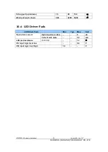
4 x pads intended for LED operation: LED[5, 2:0]
■
1 x Output on standard pad: XTAL_CLKOUT
■
1 x Power-on signaling: SYS_CTRL, usable as an input after boot.
7.2.1 PIO pad allocation
The following HSBT3031-08 functions have specific pad allocations:
■
LED pads
■
Transaction bridge
■
Audio I
²
S/PCM
NOTE Digital microphones, SPDIF, UART, Bit Serializer (I
²
C/SPI), and LED PWM controllers
can use any PIO.
7.2.2 Standard I/O
The standard digital I/O pins (PIO) on HSBT3031-08 are split into separate pad domains. Each
VDD_PADS domain can be separately powered, from 1.7 V to 3.6 V. When PIOs in a supply
domain are used for a high-speed interface, decoupling the respective VDD_PADS pin with a


