0
Features
218 programs present
Multiple picture & volume modes
On/off timer
Child-lock Program scan
Slide curtain power on/off display
DVD component input
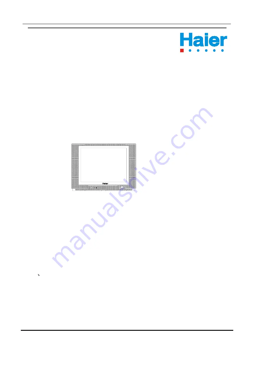
HP-2999
COLOUR TELEVISION
Service Manual
MODEL :
HP-2999
THAILAND
Manual code: M-AS-TH-HP-2999-9363 Edition: 2003.0222
Haier Group


