


3 Development Board Circuit
3.12 AD/DA
DBUG375-1.2E
22(34)
3.12
AD/DA
3.12.1
Introduction
The AD/DA module uses a chip that is a 12-bit A/D and D/A converter
with configurable 8-channel interface, which can be configured as any
combination of ADC/DAC/GPIO and shares the I2C bus with the RTC
module. The input and output interface uses 8pin, and the connection
diagram is follows.
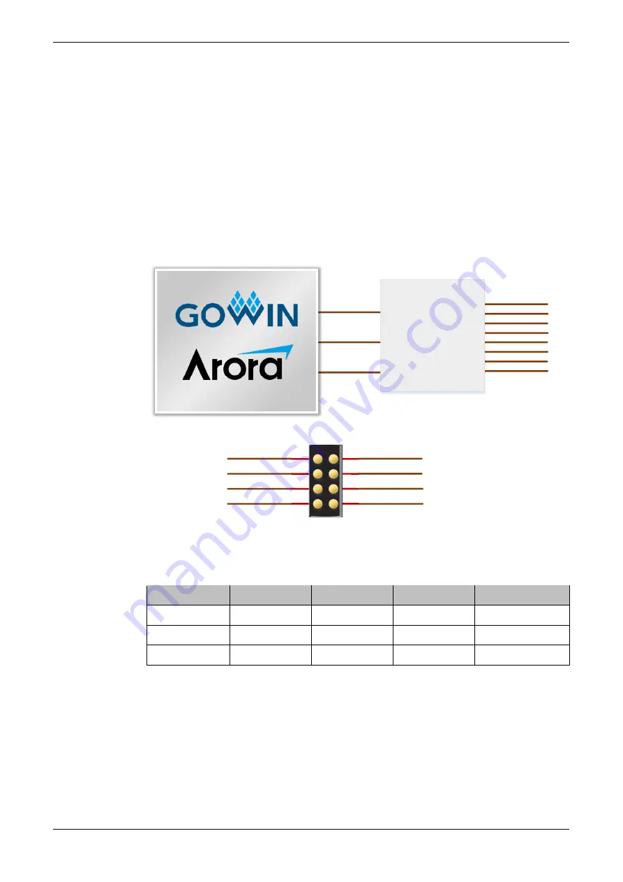
Figure 3-12 Connection Diagram of AD/DA
IIC_SDA
RTC_CLK
AD/DA_A0
AD/DA_D0
AD/DA_D1
AD/DA_D2
AD/DA_D3
AD/DA_D4
AD/DA_D5
AD/DA_D6
AD/DA_D7
AD/DA
Module
1
3
5
7
2
4
6
8
AD/DA_D0
AD/DA_D1
AD/DA_D2
AD/DA_D3
AD/DA_D4
AD/DA_D5
AD/DA_D6
AD/DA_D7
3.12.2
Pinout
Table 3-14 AD/DA Pinout
Name
FPGA Pin No. BANK
I/O Level
Description
AD/DA_A0
E14
1
2.5V
Address input
IIC_SCL
A13
1
2.5V
I2C signal
IIC_SDA
C13
1
2.5V
I2C signal
3.13
CAN
3.13.1
Introduction
The FPGA communicates with the transceiver via the UART interface,
and the maximum transmission rate is 1Mbps. The connection diagram is
as follows.


