All Rights reserved, No Spreading without GOSUNCN Permission
50
Hardware Development Guide
ME3616
7.
SMT
P
ROCESS AND
B
AKING
G
UIDE
This chapter describes module’s storage, PAD design, SMT process parameters, baking requirements, etc., and it is applicable
for the process guide to second-level assembly of LCC encapsulation module.
7.1.
S
TORAGE
R
EQUIREMENTS
Storage conditions: temperature<40
℃
, relative humidity<90% (RH), 12 months weld ability guaranteed under this
circumstances of excellent sealing package.
The Moisture sensitivity level for all modules is level 3 (Conforming to IPC/JEDEC J-STD-020). After opening the package, mount
within 168 hours under the environment conditions of temperature<30
℃
, relative humidity<60% (RH). If it doesn’t meet the above
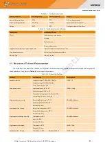
requirements, perform the baking process. See the baking parameters in Table below:
Table 7-1 Baking parameters
Temperature
Baking conditions
Baking time
Remarks
125± 5
℃
Moisture: ≤60%RH
8 hours
The accumulated baking time must be less than 96 hours
45± 5
℃
Moisture: ≤5%RH
192 hours
The product’s transportation, storage and processing must conform to IPC/JEDEC J-STD-033
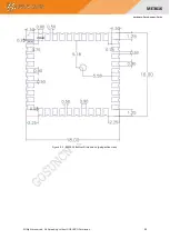
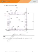
When in the process of PAD designing of module, refer to IPC-SM-782A and the chapter 6.2 below.
7.2.
M
ODULE
P
LAINNESS
S
TANDARD
Plainness of the module is required to be less than 0.15mm.
Measurement method:
put the module on the marble plane, use the feeler gage to measure the gap width at the position of
maximum warp, and do not exert force on the module during the measurement.
7.3.
P
ROCESS
R
OUTING
S
ELECTION
The modules are manufactured with the lead-free process and meet the ROHS requirements, therefore it’s recommended to
follow the lead-free manufacturing process upon the selection of process routing for module board and main board.
7.3.1.
S
OLDER
P
ASTE
S
ELECTION
The solder pastes with metal particle TYPE3 and TYPE4 can fulfill the welding requirements. It is accordingly recommended to
use the no-clean solder paste. If the solder paste which needs cleaning is used, we cannot guarantee the components on the module
board could withstand the washing of the cleaning solvents. This might cause the functional problems of such components and affect
the appearance of the module. During the printing process, make sure the solder paste’s thickness at the position of module’s PAD is
within 0.18mm~0.20mm.
7.3.2.
D
ESIGN OF MODULE
PAD’
S STEEL MESH OPENING ON MAIN BOARD
The thickness of the steel mesh on main board is selected according to the encapsulation type of components on the main
board. Pay attention to the following requirements:
Make sure to design the module PAD on main board according to chapter 5.
The thickness of steel mesh is 0.15mm or 0.18mm, but the thickness at the position of module pad can be increased to
0.18~0.20mm or the thickness of steel mesh is directly 0.18mm~0.20mm on main board.

