


GD32L23x User Manual
84
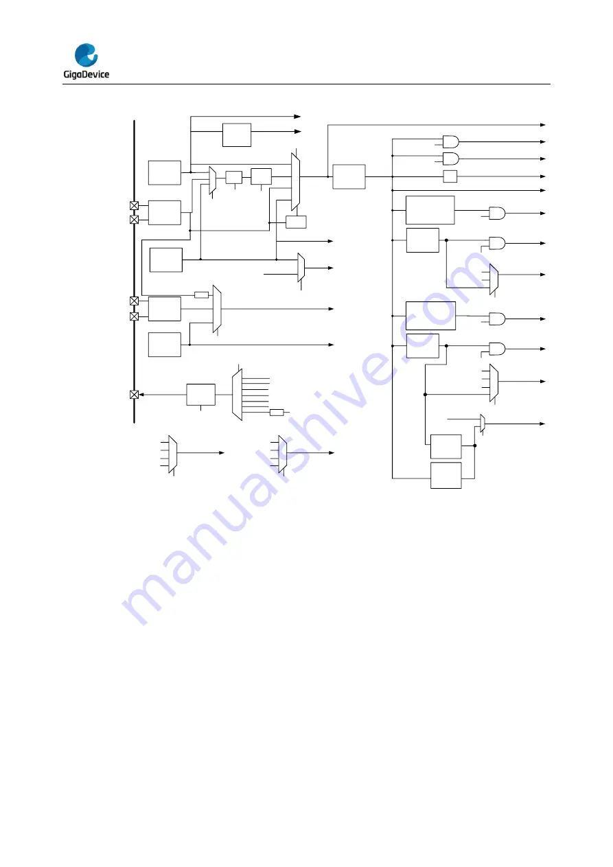
Figure 4-2. Clock tree
4-32 MHz
HXTAL
16 MHz
IRC16M
Clock
Monit or
PLLSEL[
1:0]
PREDV[3:0]
00
01
00
01
10
CK_IRC16M
CK_HXTAL
CK_PLL
CK_SYS
64 MHz max
AHB
Prescaler
÷
1,2,4,...512
CK_AHB
64 MHz max
APB1
Prescaler
÷
1,2,4,8,16
APB2
Prescaler
÷
1,2,4,8,16
CK_APB2
64 MHz max
Peripheral enable
PCLK2
to APB2 peripherals
CK_APB1
32 MHz max
Peripheral enable
PCLK1
to APB1 peripherals
TIMER8
enable
CK_TIMER8
to TIMER8
TIMERx
enable
CK_TIMERx
to TIMER1,2,5,6,11
AHB enable
HCLK
(to AHB bus,Cortex-M23,SRAM,DMA)
FMC enable
(by hardware)
CK_FMC
(to FMC)
÷8
CK_CST
(to Cortex-M23 SysTick)
FCLK
(free running clock)
32.768 KHz
LXTAL
11
10
01
32 KHz
IRC32K
CK_RTC/CK_SLCD
CK_FWDGT
(to RTC/SLCD)
(to FWDGT)
/32
CK_ LXTAL
CK_PLL
CK_HXTAL
CK_IRC16M
CK_OUT
SCS[1:0]
RTCSRC[1:0]
÷1,2.
..16
CK_I2S
(to I2S)
CK_SYS
CK_IRC32K
CK_IRC48M
/1,2
÷1,2,4...128
CKOUTDIV[2:0]
FMC
CKOUTSEL[2:0]
_
CK SYS
10
01
00
11
CK_ ADC to ADC
MHz max
ADCSEL
1
0
ADC
Prescaler
÷
,
3 5,
ADC
Prescaler
÷
,
2 4, ,
6 8
7,9
USART0SEL[1:0]
X4,5
,
,127
PLL
PLLMF
[6:0]
CK_SYS
1x
01
00
CK_I2Cx
to I2C0,1,2
I2CxSEL[1:0]
CK_IRC16M
DIV
TIMER1,2,5,6,11
if(
APB1 prescaler = 1
)
÷1
else
÷
[APB1 prescaler/2]
TIMER8
if(
APB2 prescaler = 1
)
÷1
else
÷
[APB2 prescaler/2]
11
IRC48MHz
0
1
CK_PLL
CK_USBD/CK_TRNG
(to USBD/TRNG)
USBSEL
001
010
011
100
101
110
111
CK_IRC16MDI V
CK_LXTAL
CK_IRC16M
CK_USART0
to USART0
10
01
00
11
USART1SEL/LPUS
ARTSEL[1:0]
CK_IRC16M
DIV
CK_LXTAL
CK_USART1SE
L/CK_LPUART
to USART1/LPUART
CK_SYS
CK_APB1
10
01
00
11
LPTIMERSEL[1:0]
CK_IRC16M
DIV
CK_LXTAL
CK_LPTIMER
to LPTIMER
CK_IRC32K
CK_APB2
16
10,12,14,16
11,13,15,17
1x
IRC16M
divide
÷
1,2,4,8,16
CK_IRC1
6MDI V
CK_CTC
(to CTC)
The frequency of AHB, APB2 and the APB1 domains can be configured by each prescaler.
The maximum frequency of the AHB, APB2 and APB1 domains is
64MHz/64MHz/32MHz.
The Cortex System Timer (SysTick) external clock is clocked with the AHB clock (HCLK)
divided by 8. The SysTick can work either with this clock or with the AHB clock (HCLK),
configurable in the SysTick control and status register.
The ADC are clocked by the clock of APB2 divided by 2, 4, 6, 8,10,12,14,16 or by the clock
of AHB divided by 3, 5, 7, 9,11,13,15,17 or IRC16M clock for GD32L23x series selected by
ADCSEL bit in configuration register 2 (RCU_CFG2). The USART0 is clocked by IRC16MDIV
clock or LXTAL clock or system clock or APB2 clock, which selected by USART0SEL bits in
configuration register 2 (RCU_CFG2). The USART1 is clocked by IRC16MDIV clock or LXTAL
clock or system clock or APB1 clock, which selected by USART1SEL bits in configuration
register 2 (RCU_CFG2). The LPUART is clocked by IRC16MDIV clock or LXTAL clock or
system clock or APB1 clock, which selected by LPUARTSEL bits in configuration register 2
(RCU_CFG2). The I2Cx(x=0, 1, 2) is clocked by IRC16MDIV clock or system clock or APB1
clock, which selected by I2CxSEL(x=0, 1, 2) bits in configuration register 2 (RCU_CFG2).
The RTC is clocked by LXTAL clock or IRC32K clock or HXTAL clock divided by 32 which
select by RTCSRC bits in Backup Domain Control Register (RCU_BDCTL).


