


GD32F403xx User Manual
323
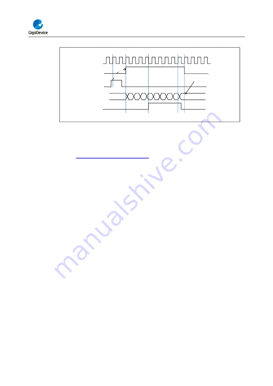
Figure 16-44. Single pulse mode TIMERx_CHxCV = 0x04 TIMERx_CAR=0x60
TIMER_CK(CNT_CLK)
CEN
CNT_REG
00
01
02
03
04
05
…
.
5F
60
00
O2CPRE
CI3
Under SPM, count er stop
Timers interconnection
Ref er to
Advanced timer (TIMERx, x=0, 7).
Timer DMA mode
Timer’s DMA mode is the function that configures timer’s register by DMA module. The relative
registers are TIMERx_DMACFG and TIMERx_DMATB; Of course, you have to enable a DMA
request which will be asserted by some internal interrupt event. When the interrupt event was
asserted, TIMERx will send a request to DMA, which is configured to M2P mode and PADDR
is TIMERx_DMATB, then DMA will access the TIMERx_DMATB. In fact, register
TIMERx_DMATB is only a buffer; timer will map the TIMERx_DMATB to an internal register,
appointed by the field of DMATA in TIMERx_DMACFG . If the field of DMATC in
TIMERx_DMACFG is 0(1 transfer), then the timer’s DMA request is finished. While if
TIMERx_DMATC is not 0, such as 3( 4 transfers), then timer will send 3 more requests to
DMA, and DMA will access timer’s registers 0x4, 0x8, 0xc
at the next 3 accesses to TIMERx_DMATB. In one word, one time DMA internal interrupt
event assert, DMATC+1 times request will be send by TIMERx.
If one more time DMA request event coming, TIMERx will repeat the process as above.
Timer debug mode
When the Cortex
®
-M4 halted, and the TIMERx_HOLD configuration bit in DBG_CTL0 register
set to 1, the TIMERx counter stops.