background image


Rev NR 


2.1.6


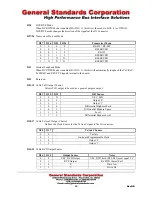
Channel RX Almost Flags: Local Offset 0x0014 / 0x0024 / 0x0034 / 0x0044 

 
The Rx Almost Flag Registers are used to set the Almost Full and Almost Empty Flags for the transmit FIFOs.  The 
Almost Full/Empty Flags may be read as status bits in the Channel Control/Status Register, and are also edge-
triggered interrupt sources to the Interrupt Register. 
 

D31:16   

 RX Almost Full Flag Value 

Number of words from FIFO Full when the Almost Full Flag will be asserted  (i.e. 
FIFO contains {FIFO Size – Almost Full Value} words or more.)  

D15:0   

 RX Almost Empty Flag Value 

Number of words from FIFO Empty when the Almost Empty Flag will be asserted  


2.1.7


Channel FIFO: Local Offset 0x0018 / 0x0028 / 0x0038 / 0x0048 

 
The Channel FIFO Register passes serial data to/from the serial controller.  The same register is used to access both 
the Transmit FIFO (writes) and Receive FIFO (reads). 
 

D31:8   

 RESERVED  

D7:0 


 Channel FIFO Data  


2.1.8


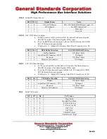
Channel Control/Status: Local Offset 0x001C / 0x002C / 0x003C / 0x004C 

 
The Channel Control/Status Register provides the reset functions and data transceiver enable controls, and the FIFO 
Flag status for each channel. 
 

D31:24  


RESERVED 

D23:20 


LED Control


Each Channel controls 2 LEDs on the back of the PCB.  See Section 5.3 for more detailed 
information about the LEDs. 

D19  


RESERVED 


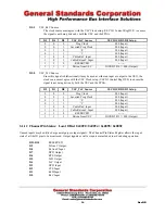
D18:8    Channel Status Bits 

D18


Rx FIFO Underflow 

D17


Tx FIFO Overflow (Latched) 

D16


Rx FIFO Overflow (Latched) 


1= Rx Data was lost due to Rx Overflow. 


Note:

   This bit is latched.  Write D16=1 to clear. 

D15


Rx FIFO Full Flag Lo 


(0 = Rx FIFO Full) 

D14


Rx FIFO Almost Full Flag Lo 


(0 = Rx FIFO Almost Full) 

D13


Rx FIFO Almost Empty Flag Lo 


(0 = Rx FIFO Almost Empty) 

D12


Rx FIFO Empty Flag Lo   


(0 = Rx FIFO Empty) 

D11


Tx FIFO Full Flag Lo 


(0 = Tx FIFO Full) 

D10


Tx FIFO Almost Full Flag Lo 


(0 = Tx FIFO Almost Full) 

D9


Tx FIFO Almost Empty Flag Lo 


(0 = Tx FIFO Almost Empty) 

D8


Tx FIFO Empty Flag Lo   


(0 = Tx FIFO Empty) 


Summary of Contents for PCIe4-SIO8BX2

Page 1: ...S232 SOFTWARE CONFIGURABLE TRANSCEIVERS AND 32K BYTE FIFO BUFFERS 512K BYTE TOTAL RS 485 RS 422 V 11 RS 232 V 28 General Standards Corporation 8302A Whitesburg Drive Huntsville AL 35802 Phone 256 880...

Page 2: ...Corporation assumes no responsibility for any errors that may exist in this document No commitment is made to update or keep current the information contained in this document General Standards Corpor...

Page 3: ...ge Digital Interface Circuits EIA order number EIA RS 422A EIA 485 Standard for Electrical Characteristics of Generators and Receivers for Use in Balanced Digital Multipoint Systems EIA order number E...

Page 4: ...03C 0X004C 8 2 1 9 CHANNEL SYNC DETECT BYTE LOCAL OFFSET 0X0050 0X0054 0X0058 0X005C 9 2 1 10 INTERRUPT REGISTERS 9 2 1 10 1 INTERRUPT CONTROL LOCAL OFFSET 0X0060 10 2 1 10 2 INTERRUPT STATUS CLEAR LO...

Page 5: ...1 1 PCI CONFIGURATION REGISTERS 26 4 1 2 LOCAL CONFIGURATION REGISTERS 27 4 1 3 RUNTIME REGISTERS 27 4 1 4 DMA REGISTERS 27 4 1 4 1 DMA CHANNEL MODE REGISTER PCI 0X80 0X94 27 CHAPTER 5 HARDWARE CONFI...

Page 6: ...ent RS422 RS485 RS232 Serial Channels Serial Mode Protocols include Asynchronous Monosync Bisync SDLC HDLC Nine Bit and IEEE 802 3 Synchronous Serial Data Rates up to 10Mbps Asynchronous Serial Data R...

Page 7: ...ls The USC provides many advanced features including Completely independent transmitter and receiver operation Odd Even Space Mark parity Two 16 bit or one 32 bit CRC polynomial Eight Data Encoding me...

Page 8: ...sfers to efficiently move data to and from the board 1 5 General Purpose IO Since some signals may not be used in all applications the SIO8BX2 provides the flexibility to remap unused signals to be us...

Page 9: ...0x0340 0x03FF Reserved 0x0400 0x043F 0x0400 Channel 4 USC Registers The GSC Firmware Registers are detailed in Section 2 1 The USC Registers are briefly touched on in Section 2 2 of this manual but ar...

Page 10: ...h 3 Pin Status 000000XX 0x009C D32 Read Only Ch 4 Pin Status 000000XX 0x00A0 D32 Read Write Programmable Osc RAM Addr 00000000 0x00A4 D32 Read Write Programmable Osc RAM Data 1 00000000 0x00A8 D32 Rea...

Page 11: ...e FIFO Write to Rx FIFO FIFO Read from Tx FIFO D28 27 FIFO Allocation Unused D26 RESERVED D25 LED D1 D6 1 Turn on Red LED D1 D6 D24 LED D1 D6 1 Turn on Green LED D1 D6 D23 Timestamp Clear 0 timestamp...

Page 12: ...th firmware rev 106 The timestamp will add a 24 bit timestamp value for each data value in the data stream Timestamp is controlled D31 24 RESERVED D23 0 Current timestamp value 2 1 5 Channel TX Almost...

Page 13: ...IFO writes and Receive FIFO reads D31 8 RESERVED D7 0 Channel FIFO Data 2 1 8 Channel Control Status Local Offset 0x001C 0x002C 0x003C 0x004C The Channel Control Status Register provides the reset fun...

Page 14: ...est Channel Sync Detect IRQ will be generated The interrupt source must be enabled in the Interrupt Control Register in order for an interrupt to be generated 2 1 10 Interrupt Registers There are 32 o...

Page 15: ...d the interrupt will occur when the FIFO transitions from NOT EMPTY to EMPTY Likewise if Tx FIFO Empty Interrupt is set as Falling Edge Triggered the interrupt will occur when the FIFO transitions fro...

Page 16: ...figures the Output source for the Clocks Data RTS and DCD outputs 31 30 29 28 27 26 25 24 Transceiver Enable Termination Disable Loopback Enable DCE DTE Mode Transceiver Protocol Mode 23 22 21 20 19 1...

Page 17: ...ignals internal to the board D22 Reserved D21 19 Cable TxD Output Control Allows TxD output to be used as a general purpose output D21 D20 D19 TxD Source 0 0 X USC_TxD 0 0 0 Output 0 0 1 1 Output 1 1...

Page 18: ...t from IO Connector DCD 0X Input 1 0 Reserved XX Don t Care 1 1 Output to IO Connector 1X Output D10 9 USC_CTS Direction Setup If CTS is used as GPIO set this field to 00 and set Pin Source Register D...

Page 19: ...SC IO Control Reg D2 0 to ensure the signal is not being driven by both the USC and the FPGA D2 D1 D0 USC_TxC Source USC IOCR D5 D3 Setup 0 0 0 Prog Clock 000 Input 0 0 1 Inverted Prog Clock 000 Input...

Page 20: ...15 0 Number of words in Tx FIFO 2 1 15 FIFO Size Register Local Offset 0x00E0 0x00E4 0x00E8 0x00EC The FIFO Size Registers display the sizes of the installed data FIFOs This value is calculated at pow...

Page 21: ...r s Manual These manuals may be obtained directly from Zilog www zilog com or copies of these manuals may be downloaded from the General Standards website www generalstandards com Some specific setup...

Page 22: ...nce the user interface to the USC is an 8 bit interface the software only needs to set the lower byte to 0x00 hardware implementation will program the upper byte of the BCR 2 2 3 USC Data Transfer Alt...

Page 23: ...R Hi Lo Channel Control Register 0x11 0x10 CMCR Hi Lo Clock Mode Control Register 0x13 0x12 HCR Hi Lo Hardware Configuration Register 0x17 0x16 IOCR Hi Lo I O Control Register 0x19 0x18 ICR Hi Lo Inte...

Page 24: ...Channel Reset The FIFO resets allow each individual FIFO Tx and Rx to be reset independently Setting the FIFO reset bit will clear the FIFO immediately 3 2 FIFOs Deep transmit and receive FIFOs are t...

Page 25: ...O counters report the exact number of data words currently in each FIFO By utilizing this information the user can determine the exact amount of data which can safely be transferred to the transmit FI...

Page 26: ...LL with postdivider per channel This allows each channel to have a unique programmable clock ProgClk The IO Connector Clocks consist of a Receive Clock RxC a Transmit Clock TxC and a bidirectional Aux...

Page 27: ...method will be to program the channel programmable clock to be 16 32 64 times the desired baudrate and use this clock as the source for the TxC RxC pin Section 2 1 11 describes how to program the Pin...

Page 28: ...ut configuration for each signal The DCD and AuxC direction is set in the Pin Source register fields independent of DCE DTE mode Signal DTE DCE TxC TxC Out RxC In RxC RxC In TxC Out TxD TxD Out RxD In...

Page 29: ...I9056 interrupts The single Local Interrupt is made up of the interrupt sources described in Section 2 1 10 In addition the Zilog USC contains a number of interrupt sources which are combined into a s...

Page 30: ...may be used to determine how much space is available for DMA so that the FIFO will never over under run Demand Mode DMA requires less software control but runs the risk of losing data due to an incom...

Page 31: ...pts to filter the information from the PCI9056 manual to provide the necessary information for a SIO8BX2 specific driver The SIO8BX2 uses an on board serial EEPROM to initialize many of the PCI9056 re...

Page 32: ...I 0x80 0x94 The DMA Channel Mode register must be setup to match the hardware implementation Bit Description Value Notes D1 0 Local Bus Width 11 32 bit 00 8 bit Although the serial FIFOs only contain...

Page 33: ...er J1 Jumper J1 allows the user to set the Board ID in the GSC Board Status Register See Section 2 1 3 This is useful to uniquely identify a board if more than one SIO8BX2 card is in a system When the...

Page 34: ...d 5 3 LEDs Ten green LEDs D1 D10 are accessible via software five to each 4 channel board Refer to Figure 5 2 for these LED locations LED D1 D6 is controlled from the Board Control Register LED D1 D6...

Page 35: ...2 TXC2 RXC2 TXC2 67 TXD2 RXD2 TXD2 RXD2 15 AUXC2 Unused Hi 66 RXD2 TXD2 Unused Hi 16 AUXC2 AUXC2 65 RXD2 TXD2 RXD2 TXD2 17 Unused Unused 64 DCD2 Unused Hi 18 Unused Unused 63 DCD2 DCD2 19 RTS2 CTS2 Un...

Page 36: ...RXD4 TXD4 145 AUXC4 AUXC4 97 DCD4 Unused Hi 144 Unused Unused 98 DCD4 DCD4 143 Unused Unused 99 CTS4 RTS4 Unused Hi 142 RTS4 CTS4 Unused Hi 100 CTS4 RTS4 CTS4 RTS4 141 RTS4 CTS4 RTS4 CTS4 101 TXD7 RX...

Page 37: ...specific application A standard cable is available which will breakout the serial channels into eight DB25 connectors Shielded cable options are also available Please consult our sales department for...

Page 38: ...ur clocks To implement this a second CLOCK RAM block was added CLOCK RAM1 programs the first CY22393 using CLKA Ch1_Clk CLKB Ch2_Clk CLKC Ch3_Clk and CLOCK_RAM2 programs the second CY22393 using CLKD...

Page 39: ...ck from the programmable oscillator to provide for slow baud rates Each 4 bit field will allow a post divider of 2 n For example if the post divider value 0 the input clock is not post divided A value...

Page 40: ...ved 0x00 0x1A Reserved 0xE9 0x1B Reserved 0x08 0x1C 0x3F Reserved Unused 0x00 0x40 PLL1 Q Setup0 0x00 0x41 PLL1 P Lo 0 Setup0 0x00 0x41 PLL1 Enable PLL1 P Hi Setup0 0x00 0x43 PLL1 Q Setup1 0x00 0x44 P...

Page 41: ...000101 D31 16 HW Board Rev 0xE00 PCIe4 SIO8BX2 Rev NR D31 1 Features Register Present D30 1 Complies with this standard D29 1 66MHz PCI bus interface 0 33MHz PCI bus interface D28 1 64 bit PCI bus int...

Page 42: ...Pin Source Change 0x02 Multi Protocol support 0x03 Common Internal External FIFO Support 0x04 FIFO Latched Underrun Overrun Level 0x05 Demand mode DMA Single Cycle for Tx 0x06 DMA_Single_Cycle_Dis up...

Reviews: