GE Multilin
C70 Capacitor Bank Protection and Control System
B-29
APPENDIX B
B.4 MEMORY MAPPING
B
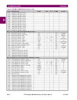
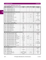
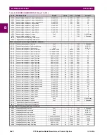
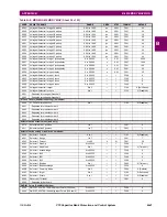
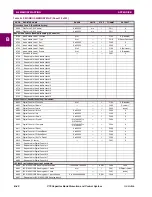
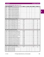
6324
Bank phase overvoltage 1 curve
0 to 3
---
1
F094
0 (FlexCurve A)
6325
Bank phase overvoltage 1 curve time multiplier
1.00 to 10.00
---
0.01
F001
100
6326
Bank phase overvoltage 1 stage 1A pickup
0.800 to 2.000
pu
0.001
F001
1050
6327
Bank phase overvoltage 1 stage 2A pickup
0.800 to 2.000
pu
0.001
F001
1100
6328
Bank phase overvoltage 1 stage 3A pickup
0.800 to 2.000
pu
0.001
F001
1200
6329
Bank phase overvoltage 1 stage 4A pickup
0.800 to 2.000
pu
0.001
F001
1050
632A
Bank phase overvoltage 1 stage 1B pickup
0.800 to 2.000
pu
0.001
F001
1050
632B
Bank phase overvoltage 1 stage 2B pickup
0.800 to 2.000
pu
0.001
F001
1100
632C
Bank phase overvoltage 1 stage 3B pickup
0.800 to 2.000
pu
0.001
F001
1200
632D
Bank phase overvoltage 1 stage 4B pickup
0.800 to 2.000
pu
0.001
F001
1050
632E
Bank phase overvoltage 1 stage 1C pickup
0.800 to 2.000
pu
0.001
F001
1050
632F
Bank phase overvoltage 1 stage 2C pickup
0.800 to 2.000
pu
0.001
F001
1100
6330
Bank phase overvoltage 1 stage 3C pickup
0.800 to 2.000
pu
0.001
F001
1200
6331
Bank phase overvoltage 1 stage 4C pickup
0.800 to 2.000
pu
0.001
F001
1050
6332
Bank phase overvoltage 1 stage 1 pickup delay
0 to 600.00
s
0.01
F001
6000
6333
Bank phase overvoltage 1 stage 2 pickup delay
0 to 600.00
s
0.01
F001
1000
6334
Bank phase overvoltage 1 stage 3 pickup delay
0 to 600.00
s
0.01
F001
200
6335
Bank phase overvoltage 1 dropout delay
0 to 600.00
s
0.01
F001
25
6336
Bank phase overvoltage 1 block
0 to 65535
---
1
F300
0
6337
Bank phase overvoltage 1 target
0 to 2
---
1
F109
0 (Self-reset)
6338
Bank phase overvoltage 1 events
0 to 1
---
1
F102
0 (Disabled)
6339
...Repeated for bank phase overvoltage 2
6352
...Repeated for bank phase overvoltage 3
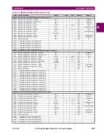
Capacitor bank overvoltage actual values (read only, 3 modules)
636B
Bank overvoltage 1 phase A operate voltage
0 to 65.535
pu
0.001
F001
0
636C
Bank overvoltage 1 phase B operate voltage
0 to 65.535
pu
0.001
F001
0
636D
Bank overvoltage 1 phase C operate voltage
0 to 65.535
pu
0.001
F001
0
636E
...Repeated for bank phase overvoltage 2
6371
...Repeated for bank phase overvoltage 3
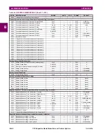
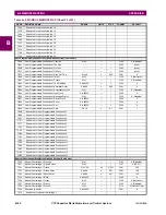
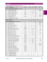
Negative Sequence Instantaneous Overcurrent (Read/Write Grouped Setting) (2 modules)
6400
Negative Sequence Instantaneous OC 1 Function
0 to 1
---
1
F102
0 (Disabled)
6401
Negative Sequence Instantaneous OC 1 Signal Source
0 to 5
---
1
F167
0 (SRC 1)
6402
Negative Sequence Instantaneous Overcurrent 1 Pickup
0 to 30
pu
0.001
F001
1000
6403
Negative Sequence Instantaneous Overcurrent 1 Delay
0 to 600
s
0.01
F001
0
6404
Negative Sequence Instantaneous OC 1 Reset Delay
0 to 600
s
0.01
F001
0
6405
Negative Sequence Instantaneous Overcurrent 1 Block
0 to 65535
---
1
F300
0
6406
Negative Sequence Instantaneous Overcurrent 1 Target
0 to 2
---
1
F109
0 (Self-reset)
6407
Negative Sequence Instantaneous Overcurrent 1 Events
0 to 1
---
1
F102
0 (Disabled)
6408
Reserved (8 items)
0 to 1
---
1
F001
0
6410
...Repeated for Negative Sequence Instantaneous OC 2
Negative Sequence Overvoltage (Read/Write Grouped Setting)
64A0
Negative Sequence Overvoltage Function
0 to 1
---
1
F102
0 (Disabled)
64A1
Negative Sequence Overvoltage Source
0 to 5
---
1
F167
0 (SRC 1)
64A2
Negative Sequence Overvoltage Pickup
0 to 1.25
pu
0.001
F001
300
64A3
Negative Sequence Overvoltage Pickup Delay
0 to 600
s
0.01
F001
50
64A4
Negative Sequence Overvoltage Reset Delay
0 to 600
s
0.01
F001
50
64A5
Negative Sequence Overvoltage Block
0 to 65535
---
1
F300
0
64A6
Negative Sequence Overvoltage Target
0 to 2
---
1
F109
0 (Self-reset)
64A7
Negative Sequence Overvoltage Events
0 to 1
---
1
F102
0 (Disabled)
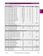
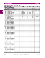
Time of day timer settings (read/write, grouped, 5 modules)
6570
Time of day timer 1 function
0 to 1
---
1
F102
0 (Disabled)
6571
Time of day timer 1 start time
0 to 2359
---
1
F050
0
6573
Time of day timer 1 stop time
0 to 2359
---
1
F001
2359
6575
Time of day timer 1 targets
0 to 2
---
1
F109
0 (Self-reset)
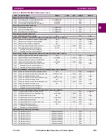
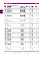
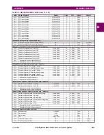
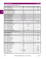
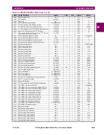
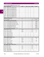
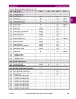
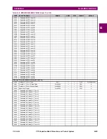
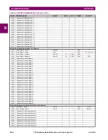
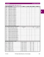
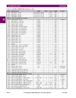
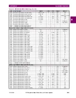
Table B–9: MODBUS MEMORY MAP (Sheet 22 of 53)
ADDR
REGISTER NAME
RANGE
UNITS
STEP
FORMAT
DEFAULT
Summary of Contents for UR Series C70
Page 2: ......
Page 10: ...x C70 Capacitor Bank Protection and Control System GE Multilin TABLE OF CONTENTS ...
Page 344: ...5 220 C70 Capacitor Bank Protection and Control System GE Multilin 5 10 TESTING 5 SETTINGS 5 ...
Page 586: ...D 10 C70 Capacitor Bank Protection and Control System GE Multilin D 1 OVERVIEW APPENDIXD D ...

