GE Multilin
C70 Capacitor Bank Protection and Control System
B-17
APPENDIX B
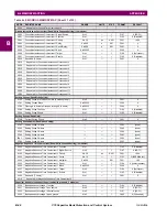
B.4 MEMORY MAPPING
B
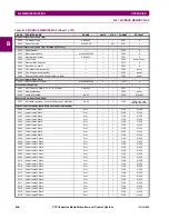
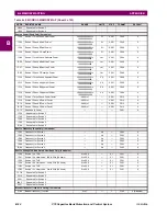
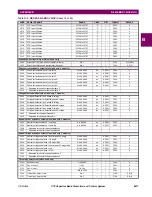
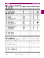
3514
RTD Input 37 Value
-32768 to 32767
°C
1
F002
0
3515
RTD Input 38 Value
-32768 to 32767
°C
1
F002
0
3516
RTD Input 39 Value
-32768 to 32767
°C
1
F002
0
3517
RTD Input 40 Value
-32768 to 32767
°C
1
F002
0
3518
RTD Input 41 Value
-32768 to 32767
°C
1
F002
0
3519
RTD Input 42 Value
-32768 to 32767
°C
1
F002
0
351A
RTD Input 43 Value
-32768 to 32767
°C
1
F002
0
351B
RTD Input 44 Value
-32768 to 32767
°C
1
F002
0
351C
RTD Input 45 Value
-32768 to 32767
°C
1
F002
0
351D
RTD Input 46 Value
-32768 to 32767
°C
1
F002
0
351E
RTD Input 47 Value
-32768 to 32767
°C
1
F002
0
351F
RTD Input 48 Value
-32768 to 32767
°C
1
F002
0
Expanded Direct Input/Output Status (Read Only)
3560
Direct Device States, one per register (8 items)
0 to 1
---
1
F155
0 (Offline)
3570
Direct Input States, one per register (96 items)
0 to 1
---
1
F108
0 (Off)
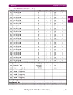
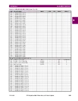
Phase current unbalance actual values (read only, 3 modules)
3600
Phase current unbalance 1 raw Idiff A
0 to 99.9999
pu
0.0001
F004
0
3602
Phase current unbalance 1 raw Idiff B
0 to 99.9999
pu
0.0001
F004
0
3604
Phase current unbalance 1 raw Idiff C
0 to 99.9999
pu
0.0001
F004
0
3606
Phase current unbalance 1 comp Iop A
0 to 99.9999
pu
0.0001
F004
0
3608
Phase current unbalance 1 comp Iop B
0 to 99.9999
pu
0.0001
F004
0
360A
Phase current unbalance 1 comp Iop C
0 to 99.9999
pu
0.0001
F004
0
360C
...Repeated for phase current unbalance 2
3618
...Repeated for phase current unbalance 3
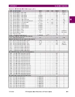
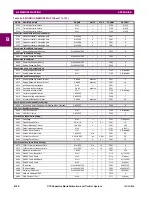
Voltage differential actual values (read only, 3 modules)
3640
Voltage differential 1 bus phase A voltage
0 to 99.9999
pu
0.0001
F003
0
3642
Voltage differential 1 differential phase A voltage
0 to 99.9999
pu
0.0001
F003
0
3644
Voltage differential 1 bus phase B voltage
0 to 99.9999
pu
0.0001
F003
0
3646
Voltage differential 1 differential phase B voltage
0 to 99.9999
pu
0.0001
F003
0
3648
Voltage differential 1 bus phase C voltage
0 to 99.9999
pu
0.0001
F003
0
364A
Voltage differential 1 differential phase C voltage
0 to 99.9999
pu
0.0001
F003
0
364C
...Repeated for voltage differential 2
3658
...Repeated for voltage differential 3
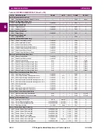
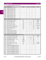
Neutral current unbalance actual values (read only, 3 modules)
36C4
Neutral current unbalance 1 raw INsp
0 to 9.9999
pu
0.0001
F003
0
36C6
Neutral current unbalance 1 comp Iop
0 to 9.9999
pu
0.0001
F003
0
36C8
...Repeated for neutral current unbalance 2
36CC
...Repeated for neutral current unbalance 3
Neutral voltage unbalance actual values (read only, 3 modules)
36F0
Neutral voltage unbalance 1 neutral point Vx angle
0 to 99.9999
°
0.0001
F004
0
36F2
Neutral voltage unbalance 1 V0 angle
0 to 99.9999
°
0.0001
F004
0
36F4
Neutral voltage unbalance 1 V0 magnitude
0 to 99.9999
pu
0.0001
F004
0
36F6
Neutral voltage unbalance 1 neutral point Vx magnitude
0 to 99.9999
pu
0.0001
F004
0
36F8
Neutral voltage unbalance 1 Vop
0 to 99.9999
pu
0.0001
F004
0
36FA
Neutral voltage unbalance 1 Vrest
0 to 99.9999
pu
0.0001
F004
0
36FC
...Repeated for neutral voltage unbalance 2
3708
...Repeated for neutral voltage unbalance 3
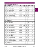
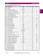
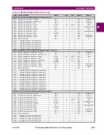
Time of day timer actual values (read only)
3720
Seconds of day
1 to 86400
---
1
F003
0
3722
Day of month
1 to 31
---
1
F001
0
3723
Day of year
1 to 366
---
1
F001
0
3724
Year
1970 to 3000
---
1
F001
0
3730
Time of day timer 1 state
0 to 1
---
1
F108
0 (Off)
3731
Time of day timer 2 state
0 to 1
---
1
F108
0 (Off)
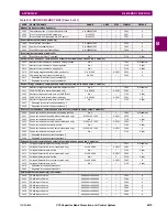
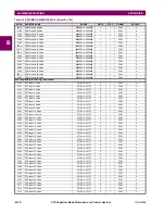
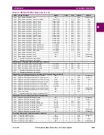
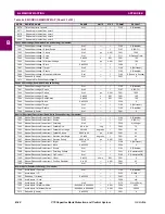
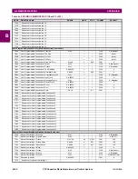
Table B–9: MODBUS MEMORY MAP (Sheet 10 of 53)
ADDR
REGISTER NAME
RANGE
UNITS
STEP
FORMAT
DEFAULT
Summary of Contents for UR Series C70
Page 2: ......
Page 10: ...x C70 Capacitor Bank Protection and Control System GE Multilin TABLE OF CONTENTS ...
Page 344: ...5 220 C70 Capacitor Bank Protection and Control System GE Multilin 5 10 TESTING 5 SETTINGS 5 ...
Page 586: ...D 10 C70 Capacitor Bank Protection and Control System GE Multilin D 1 OVERVIEW APPENDIXD D ...

