background image

5-50

C70 Capacitor Bank Protection and Control System

GE Multilin

5.2 PRODUCT SETUP

5 SETTINGS

5

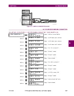
PUSHBTN 1 SET

: This setting assigns the FlexLogic™ operand serving to operate the pushbutton element and to

assert 

PUSHBUTTON 1 ON

 operand. The duration of the incoming set signal must be at least 100 ms.

PUSHBTN 1 RESET

: This setting assigns the FlexLogic™ operand serving to reset pushbutton element and to assert

PUSHBUTTON 1 OFF

 operand. This setting is applicable only if pushbutton is in latched mode. The duration of the

incoming reset signal must be at least 50 ms.

PUSHBTN 1 AUTORST

: This setting enables the user-programmable pushbutton autoreset feature. This setting is

applicable only if the pushbutton is in the “Latched” mode. 

PUSHBTN 1 AUTORST DELAY

: This setting specifies the time delay for automatic reset of the pushbutton when in

the latched mode.

PUSHBTN 1 REMOTE

: This setting assigns the FlexLogic™ operand serving to inhibit pushbutton operation from the

operand assigned to the 

PUSHBTN 1 SET

 or 

PUSHBTN 1 RESET

 settings.

PUSHBTN 1 LOCAL

: This setting assigns the FlexLogic™ operand serving to inhibit pushbutton operation from the

front panel pushbuttons. This locking functionality is not applicable to pushbutton autoreset. 

PUSHBTN 1 DROP-OUT TIME

: This setting applies only to “Self-Reset” mode and specifies the duration of the push-

button active status after the pushbutton has been released. When activated remotely, this setting specifies the entire
activation time of the pushbutton status; the length of time the operand remains on has no effect on the pulse duration.
This setting is required to set the duration of the pushbutton operating pulse.

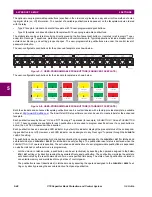
PUSHBTN 1 LED CTL

: This setting assigns the FlexLogic™ operand serving to drive pushbutton LED. If this setting is

“Off”, then LED operation is directly linked to 

PUSHBUTTON 1 ON

 operand.

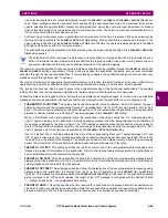
PUSHBTN 1 MESSAGE

: If pushbutton message is set to “High Priority”, the message programmed in the 

PUSHBTN 1

ID

 and 

PUSHBTN 1 ON TEXT

 settings will be displayed undisturbed as long as 

PUSHBUTTON 1 ON

 operand is asserted.

The high priority option is not applicable to the 

PUSHBTN 1 OFF TEXT

 setting.

This message can be temporary removed if any front panel keypad button is pressed. However, ten seconds of keypad
inactivity will restore the message if the 

PUSHBUTTON 1 ON

 operand is still active.

If the 

PUSHBTN 1 MESSAGE

 is set to “Normal”, the message programmed in the 

PUSHBTN 1 ID

 and 

PUSHBTN 1 ON TEXT

settings will be displayed as long as 

PUSHBUTTON 1 ON

 operand is asserted, but not longer than time period specified

by 

FLASH MESSAGE TIME

 setting. After the flash time is expired, the default message or other active target message is

displayed. The instantaneous reset of the flash message will be executed if any relay front panel button is pressed or
any new target or message becomes active.

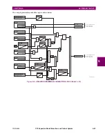
The 

PUSHBTN 1 OFF TEXT

 setting is linked to 

PUSHBUTTON 1 OFF

 operand and will be displayed in conjunction with

PUSHBTN 1 ID

 only if pushbutton element is in the “Latched” mode. The 

PUSHBTN 1 OFF TEXT

 message will be displayed

as “Normal” if the 

PUSHBTN 1 MESSAGE

 setting is “High Priority” or “Normal”.

PUSHBUTTON 1 EVENTS

: If this setting is enabled, each pushbutton state change will be logged as an event into

event recorder.

Summary of Contents for UR Series C70

Page 1: ... GEK 113517B Copyright 2010 GE Multilin GE Multilin 215 Anderson Avenue Markham Ontario Canada L6E 1B3 Tel 905 294 6222 Fax 905 201 2098 Internet http www GEmultilin com Title Page IISO9001 2000 G E M ULTILI N R E GISTERE D GE Multilin s Quality Management System is registered to ISO9001 2000 QMI 005094 UL A3775 1601 9015 U3 LISTED 52TL IND CONT EQ E83849 ...

Page 2: ......

Page 3: ...ARCHY 1 17 1 5 4 RELAY ACTIVATION 1 17 1 5 5 RELAY PASSWORDS 1 18 1 5 6 FLEXLOGIC CUSTOMIZATION 1 18 1 5 7 COMMISSIONING 1 19 2 PRODUCT DESCRIPTION 2 1 INTRODUCTION 2 1 1 OVERVIEW 2 1 2 1 2 ORDERING 2 3 2 1 3 REPLACEMENT MODULES 2 6 2 2 SPECIFICATIONS 2 2 1 PROTECTION ELEMENTS 2 9 2 2 2 USER PROGRAMMABLE ELEMENTS 2 12 2 2 3 MONITORING 2 13 2 2 4 METERING 2 13 2 2 5 INPUTS 2 14 2 2 6 POWER SUPPLY 2...

Page 4: ... MAIN WINDOW 4 3 4 2 EXTENDED ENERVISTA UR SETUP FEATURES 4 2 1 SETTINGS TEMPLATES 4 4 4 2 2 SECURING AND LOCKING FLEXLOGIC EQUATIONS 4 8 4 2 3 SETTINGS FILE TRACEABILITY 4 10 4 3 FACEPLATE INTERFACE 4 3 1 FACEPLATE 4 13 4 3 2 LED INDICATORS 4 14 4 3 3 CUSTOM LABELING OF LEDS 4 17 4 3 4 DISPLAY 4 22 4 3 5 KEYPAD 4 22 4 3 6 BREAKER CONTROL 4 23 4 3 7 MENUS 4 24 4 3 8 CHANGING SETTINGS 4 26 5 SETTIN...

Page 5: ...5 7 CONTROL ELEMENTS 5 7 1 OVERVIEW 5 162 5 7 2 TRIP BUS 5 162 5 7 3 SETTING GROUPS 5 164 5 7 4 SELECTOR SWITCH 5 165 5 7 5 TIME OF DAY TIMERS 5 171 5 7 6 CAPACITOR CONTROL 5 172 5 7 7 AUTOMATIC VOLTAGE REGULATOR 5 177 5 7 8 DIGITAL ELEMENTS 5 182 5 7 9 DIGITAL COUNTERS 5 185 5 7 10 MONITORING ELEMENTS 5 187 5 8 INPUTS OUTPUTS 5 8 1 CONTACT INPUTS 5 196 5 8 2 VIRTUAL INPUTS 5 198 5 8 3 CONTACT OUT...

Page 6: ...580 GOOSE ANALOG VALUES 6 19 6 3 8 TRANSDUCER INPUTS OUTPUTS 6 19 6 4 RECORDS 6 4 1 USER PROGRAMMABLE FAULT REPORTS 6 20 6 4 2 EVENT RECORDS 6 20 6 4 3 OSCILLOGRAPHY 6 20 6 4 4 DATA LOGGER 6 21 6 5 PRODUCT INFORMATION 6 5 1 MODEL INFORMATION 6 22 6 5 2 FIRMWARE REVISIONS 6 22 7 COMMANDS AND TARGETS 7 1 COMMANDS 7 1 1 COMMANDS MENU 7 1 7 1 2 CAPACITOR BANK AUTOMATIC SETTINGS 7 1 7 1 3 VIRTUAL INPUT...

Page 7: ...NNECTED BANKS 10 3 10 2 2 UNGROUNDED WYE CONNECTED BANKS 10 3 10 2 3 DELTA CONNECTED BANKS 10 3 10 2 4 H CONFIGURATION 10 3 10 2 5 TAPPED CONFIGURATION 10 3 10 2 6 SUMMARY 10 4 10 3 PROTECTION METHODS FOR CAPACITOR BANKS 10 3 1 DESCRIPTION 10 5 10 3 2 CAPACITOR UNBALANCE PROTECTION 10 5 10 3 3 PROTECTION FOR RACK FAULTS ARC OVER WITHIN CAPACITOR BANK 10 10 10 3 4 OVERVOLTAGE 10 10 10 3 5 OVERCURRE...

Page 8: ...6 MMXU ANALOG MEASURED VALUES C 3 C 2 7 PROTECTION AND OTHER LOGICAL NODES C 3 C 3 SERVER FEATURES AND CONFIGURATION C 3 1 BUFFERED UNBUFFERED REPORTING C 5 C 3 2 FILE TRANSFER C 5 C 3 3 TIMESTAMPS AND SCANNING C 5 C 3 4 LOGICAL DEVICE NAME C 5 C 3 5 LOCATION C 5 C 3 6 LOGICAL NODE NAME PREFIXES C 6 C 3 7 CONNECTION TIMING C 6 C 3 8 NON IEC 61850 DATA C 6 C 3 9 COMMUNICATION SOFTWARE UTILITIES C 6...

Page 9: ...ICE PROFILE DOCUMENT E 1 1 DNP V3 00 DEVICE PROFILE E 1 E 1 2 IMPLEMENTATION TABLE E 4 E 2 DNP POINT LISTS E 2 1 BINARY INPUT POINTS E 8 E 2 2 BINARY AND CONTROL RELAY OUTPUT E 9 E 2 3 COUNTERS E 10 E 2 4 ANALOG INPUTS E 11 F MISCELLANEOUS F 1 CHANGE NOTES F 1 1 REVISION HISTORY F 1 F 1 2 CHANGES TO THE C70 MANUAL F 1 F 2 ABBREVIATIONS F 2 1 STANDARD ABBREVIATIONS F 6 F 3 WARRANTY F 3 1 GE MULTILI...

Page 10: ...x C70 Capacitor Bank Protection and Control System GE Multilin TABLE OF CONTENTS ...

Page 11: ...ormation instruction manual updates and the latest software updates please visit the GE Multilin website at http www GEmultilin com If there is any noticeable physical damage or any of the contents listed are missing please contact GE Multilin immediately GE MULTILIN CONTACT INFORMATION AND CALL CENTER FOR PRODUCT SUPPORT GE Multilin 215 Anderson Avenue Markham Ontario Canada L6E 1B3 TELEPHONE 905...

Page 12: ...mount of cabling and auxiliary equipment installed in stations can be even further reduced to 20 to 70 of the levels common in 1990 to achieve large cost reductions This requires placing even more functions within the IEDs Users of power equipment are also interested in reducing cost by improving power quality and personnel productivity and as always in increasing system reliability and efficiency...

Page 13: ...tomize the device Virtual outputs can also serve as virtual inputs to FlexLogic equations The analog inputs and outputs are signals that are associated with transducers such as Resistance Temperature Detec tors RTDs The CT and VT inputs refer to analog current transformer and voltage transformer signals used to monitor AC power lines The UR series relays support 1 A and 5 A CTs The remote inputs a...

Page 14: ...used for metering input output control hmi communications or any functional entity in the system Employing OOD OOP in the software architecture of the C70 achieves the same features as the hardware architecture modularity scalability and flexibility The application software for any UR series device for example feeder protection transformer protection distance protection is constructed by combining...

Page 15: ... capable of displaying 800 x 600 or higher in high color mode 16 bit color RS232 and or Ethernet port for communications to the relay The following qualified modems have been tested to be compliant with the C70 and the EnerVista UR Setup software US Robotics external 56K FaxModem 5686 US Robotics external Sportster 56K X2 PCTEL 2304WT V 92 MDC internal modem 1 3 2 INSTALLATION After ensuring the m...

Page 16: ...n the installation The files will be installed in the directory indicated and the installation program will automatically create icons and add EnerVista UR Setup to the Windows start menu 9 Click Finish to end the installation The UR series device will be added to the list of installed IEDs in the EnerVista Launchpad window as shown below 1 3 3 CONFIGURING THE C70 FOR SOFTWARE ACCESS a OVERVIEW Th...

Page 17: ... is will be required Refer to the F485 instruction manual for additional details 1 Verify that the latest version of the EnerVista UR Setup software is installed available from the GE EnerVista CD or online from http www GEmultilin com See the Software Installation section for installation details 2 Select the UR device from the EnerVista Launchpad to start EnerVista UR Setup 3 Click the Device Se...

Page 18: ...ns it will be necessary to define a Site then add the relay as a Device at that site 1 Verify that the latest version of the EnerVista UR Setup software is installed available from the GE EnerVista CD or online from http www GEmultilin com See the Software Installation section for installation details 2 Select the UR device from the EnerVista Launchpad to start EnerVista UR Setup 3 Click the Devic...

Page 19: ...hat the latest version of the EnerVista UR Setup software is installed available from the GE EnerVista CD or online from http www GEmultilin com See the Software Installation section for installation details 2 Select the UR device from the EnerVista Launchpad to start EnerVista UR Setup 3 Click the Quick Connect button to open the Quick Connect dialog box 4 Select the Serial interface and the corr...

Page 20: ... laptop computer an IP address compatible with the relay s IP address 1 From the Windows desktop right click the My Network Places icon and select Properties to open the network con nections window 2 Right click the Local Area Connection icon and select Properties 842799A1 CDR END 1 END 2 Pin Wire color Diagram Pin Wire color Diagram 1 White orange 1 White green 2 Orange 2 Green 3 White green 3 Wh...

Page 21: ...ction 1 Open a Windows console window by selecting Start Run from the Windows Start menu and typing cmd 2 Type the following command C WINNT ping 1 1 1 1 3 If the connection is successful the system will return four replies as follows Pinging 1 1 1 1 with 32 bytes of data Reply from 1 1 1 1 bytes 32 time 10ms TTL 255 Reply from 1 1 1 1 bytes 32 time 10ms TTL 255 Reply from 1 1 1 1 bytes 32 time 10...

Page 22: ...2 bytes of data Verify the physical connection between the C70 and the laptop computer and double check the programmed IP address in the PRODUCT SETUP ÖØ COMMUNICATIONS ÖØ NETWORK Ö IP ADDRESS setting then repeat step 2 in the above procedure If the following sequence of messages appears when entering the C WINNT ping 1 1 1 1 command Pinging 1 1 1 1 with 32 bytes of data Destination host unreachab...

Page 23: ...3 Select the UR device from the EnerVista Launchpad to start EnerVista UR Setup 4 Click the Quick Connect button to open the Quick Connect dialog box 5 Select the Ethernet interface and enter the IP address assigned to the C70 then click Connect 6 The EnerVista UR Setup software will create a site named Quick Connect with a corresponding device also named Quick Connect and display them on the uppe...

Page 24: ...CES The EnerVista UR Setup software can automatically discover and communicate to all UR series IEDs located on an Ether net network Using the Quick Connect feature a single click of the mouse will trigger the software to automatically detect any UR series relays located on the network The EnerVista UR Setup software will then proceed to configure all settings and order code options in the Device ...

Page 25: ...ow be edited printed or changed according to user specifications Refer to chapter 4 in this manual and the EnerVista UR Setup Help File for more information about the using the EnerVista UR Setup software interface QUICK ACTION HOT LINKS The EnerVista UR Setup software has several new quick action buttons that provide users with instant access to several functions that are often performed when usi...

Page 26: ...32 port the GE Multilin RS232 RS485 converter box is required This device catalog number F485 connects to the computer using a straight through serial cable A shielded twisted pair 20 22 or 24 AWG connects the F485 converter to the C70 rear communications port The converter termi nals GND are connected to the C70 communication module COM terminals Refer to the CPU communica tions ports section in ...

Page 27: ... enabled 1 5 3 MENU HIERARCHY The setting and actual value messages are arranged hierarchically The header display pages are indicated by double scroll bar characters while sub header pages are indicated by single scroll bar characters The header display pages represent the highest level of the hierarchy and the sub header display pages fall below this level The MESSAGE UP and DOWN keys move withi...

Page 28: ...d to specific personnel There are two user password security access levels COMMAND and SETTING 1 COMMAND The COMMAND access level restricts the user from making any settings changes but allows the user to perform the fol lowing operations change state of virtual inputs clear event records clear oscillography records operate user programmable pushbuttons 2 SETTING The SETTING access level allows th...

Page 29: ... messages and LED indications 3 LED test 4 Visual inspection for any damage corrosion dust or loose wires 5 Event recorder file download with further events analysis Out of service maintenance 1 Check wiring connections for firmness 2 Analog values currents voltages RTDs analog inputs injection test and metering accuracy verification Calibrated test equipment is required 3 Protection elements sett...

Page 30: ...1 20 C70 Capacitor Bank Protection and Control System GE Multilin 1 5 USING THE RELAY 1 GETTING STARTED 1 ...

Page 31: ...series IEDs The C70 metering functions include true RMS and phasors for currents and voltages current and voltage harmonics and THD symmetrical components frequency power power factor Diagnostic features include an event recorder capable of storing 1024 time tagged events oscillography capable of storing up to 64 records with programmable trigger content and sampling rate and data logger acquisiti...

Page 32: ...current 59X Auxiliary overvoltage 50P Phase instantaneous overcurrent 59_2 Negative sequence overvoltage 50_2 Negative sequence instantaneous overcurrent 60N Bank neutral current unbalance 51G Ground time overcurrent 60P Bank phase current unbalance 51N Neutral time overcurrent 67N Neutral directional overcurrent 51P Phase time overcurrent 87V Bank voltage differential 51_2 Negative sequence time ...

Page 33: ...ules regu lar CT VT modules or the HardFiber modules The order code options are described in the following sub sections Table 2 2 OTHER DEVICE FUNCTIONS FUNCTION FUNCTION FUNCTION Breaker control Direct inputs and outputs 32 Time and date Breaker flashover Event recorder Time synchronization over SNTP Breaker restrike FlexElements 16 Transducer inputs and outputs Capacitor control supervision Flex...

Page 34: ...nostics DIGITAL INPUTS OUTPUTS XX XX XX No Module 6A 6A 6A 6A 6A 2 Form A voltage with optional current and 2 Form C outputs 8 digital inputs 6B 6B 6B 6B 6B 2 Form A voltage with optional current and 4 Form C outputs 4 digital inputs 6C 6C 6C 6C 6C 8 Form C outputs 6D 6D 6D 6D 6D 16 digital inputs 6E 6E 6E 6E 6E 4 Form C outputs 8 digital inputs 6F 6F 6F 6F 6F 8 Fast Form C outputs 6G 6G 6G 6G 6G ...

Page 35: ...ot P is used for digital input output modules slot R is used for inter relay communications modules 2G IEEE C37 94 820 nm 128 kbps multimode LED 1 Channel 2H IEEE C37 94 820 nm 128 kbps multimode LED 2 Channels 2S Six port managed Ethernet switch with high voltage power supply 110 to 250 V DC 100 to 240 V AC 2T Six port managed Ethernet switch with low voltage power supply 48 V DC 77 IEEE C37 94 8...

Page 36: ...rogrammable pushbuttons N Enhanced front panel with French display and user programmable pushbuttons T Enhanced front panel with Russian display and user programmable pushbuttons V Enhanced front panel with Chinese display and user programmable pushbuttons POWER SUPPLY H 125 250 V AC DC power supply L 24 to 48 V DC only power supply PROCESS BUS MODULE 81 Eight port digital process bus module DIGIT...

Page 37: ...ital inputs 6E 4 Form C outputs 8 digital inputs 6F 8 Fast Form C outputs 6G 4 Form A voltage with optional current outputs 8 digital inputs 6H 6 Form A voltage with optional current outputs 4 digital inputs 6K 4 Form C and 4 Fast Form C outputs 6L 2 Form A current with optional voltage and 2 Form C outputs 8 digital inputs 6M 2 Form A current with optional voltage and 4 Form C outputs 4 digital i...

Page 38: ...A voltage with optional current outputs 8 digital inputs 6H 6 Form A voltage with optional current outputs 4 digital inputs 6K 4 Form C and 4 Fast Form C outputs 6L 2 Form A current with optional voltage and 2 Form C outputs 8 digital inputs 6M 2 Form A current with optional voltage and 4 Form C outputs 4 digital inputs 6N 4 Form A current with optional voltage outputs 8 digital inputs 6P 6 Form A...

Page 39: ...th power factor limit Minimum voltage supervision 0 500 to 1 500 pu in steps of 0 001 Close voltage level 0 750 to 1 500 pu in steps of 0 001 Open voltage level 0 750 to 1 500 pu in steps of 0 001 Voltage pickup accuracy 0 5 of setting from 10 to 208 V Close reactive power level 1 50 to 1 50 pu in steps of 0 01 Open reactive power level 1 50 to 1 50 pu in steps of 0 01 Power pickup accuracy 0 05 p...

Page 40: ...16 ms at 3 pickup at 60 Hz PHASE CURRENT UNBALANCE Operation per phase Auto setting on demand from keypad per phase Number of elements 1 per CT bank maximum of 3 Inherent unbalance factor 0 1000 to 0 1000 in steps of 0 0001 per phase Number of trip alarm stages 4 per phase with individual timers per stage Pickup threshold 0 001 to 5 000 pu of split phase CT nom inal in steps of 0 001 Pickup level ...

Page 41: ...Y OVERVOLTAGE Pickup level 0 000 to 3 000 pu in steps of 0 001 Dropout level 97 to 98 of pickup Level accuracy 0 5 of reading from 10 to 208 V Pickup delay 0 to 600 00 s in steps of 0 01 Reset delay 0 to 600 00 s in steps of 0 01 Timing accuracy 3 of operate time or 4 ms whichever is greater Operate time 30 ms at 1 10 pickup at 60 Hz NEGATIVE SEQUENCE OVERVOLTAGE Pickup level 0 000 to 1 250 pu in ...

Page 42: ...c USER PROGRAMMABLE LEDs Number 48 plus trip and alarm Programmability from any logical variable contact or vir tual input Reset mode self reset or latched LED TEST Initiation from any digital input or user program mable condition Number of tests 3 interruptible at any time Duration of full test approximately 3 minutes Test sequence 1 all LEDs on Test sequence 2 all LEDs off one LED at a time on f...

Page 43: ...ays 2 2 4 METERING RMS CURRENT PHASE NEUTRAL AND GROUND Accuracy at 0 1 to 2 0 CT rating 0 25 of reading or 0 1 of rated whichever is greater 2 0 CT rating 1 0 of reading RMS VOLTAGE Accuracy 0 5 of reading from 10 to 208 V REAL POWER WATTS Accuracy 1 0 of reading at 0 8 PF 1 0 and 0 8 PF 1 0 REACTIVE POWER VARS Accuracy 1 0 of reading at 0 2 PF 0 2 APPARENT POWER VA Accuracy 1 0 of reading CURREN...

Page 44: ... impulse current 50 to 70 mA Duration of auto burnish impulse 25 to 50 ms DCMA INPUTS Current input mA DC 0 to 1 0 to 1 1 to 1 0 to 5 0 to 10 0 to 20 4 to 20 programmable Input impedance 379 Ω 10 Conversion range 1 to 20 mA DC Accuracy 0 2 of full scale Type Passive IRIG B INPUT Amplitude modulation 1 to 10 V pk pk DC shift TTL Input impedance 22 kΩ Isolation 2 kV REMOTE INPUTS IEC 61850 GSSE GOOS...

Page 45: ...DC inductive L R 40 ms Operate time 8 ms Contact material silver alloy FAST FORM C RELAY Make and carry 0 1 A max resistive load Minimum load impedance Operate time 0 6 ms Internal Limiting Resistor 100 Ω 2 W SOLID STATE OUTPUT RELAY Operate and release time 100 μs Maximum voltage 265 V DC Maximum continuous current 5 A at 45 C 4 A at 65 C Make and carry for 0 2 s 30 A as per ANSI C37 90 for 0 03 ...

Page 46: ... 50 60 Hz Minimum AC voltage 85 V AC 0 31 A 22 VA at 50 60 Hz Maximum AC voltage 265 V AC 0 16 A 42 VA at 50 60 Hz Internal fuse 3 A 350 V AC Ceramic Axial SLO BLO Manufacturer Conquer Part number SCD A 003 ETHERNET SWITCH LOW VOLTAGE TYPE 2T Nominal voltage 48 V DC 0 31 A 15 W Minimum voltage 30 V DC 0 43 A 16 W Maximum voltage 60 V DC Internal fuse 5 A 350 V AC Ceramic Axial SLO BLO Manufacturer...

Page 47: ...sertion loss of 1db for either direction The worst case optical power budget between two type 2T or 2S modules using a single fiber cable is To calculate the maximum fiber length divide the worst case opti cal power budget by the cable attenuation per unit distance speci fied in the manufacturer data sheets For example typical attenuation for 62 5 125 μm glass fiber optic cable is approxi mately 2...

Page 48: ...sing at 55 C as per IEC60068 2 30 variant 1 6days OTHER Altitude 2000 m maximum Pollution degree II Overvoltage category II Ingress protection IP20 front IP10 back INTERFACE TYPE TYPICAL DISTANCE RS422 1200 m G 703 100 m EMITTER FIBER TYPE TRANSMIT POWER RECEIVED SENSITIVITY POWER BUDGET 820 nm LED Multimode 20 dBm 30 dBm 10 dB 1300 nm LED Multimode 21 dBm 30 dBm 9 dB 1300 nm ELED Singlemode 23 dB...

Page 49: ...22 7 Class A and B Voltage interruption and ripple DC IEC60255 11 12 ripple 200 ms interrupts Radiated and conducted emissions CISPR11 CISPR22 IEC60255 25 Class A Sinusoidal vibration IEC60255 21 1 Class 1 Shock and bump IEC60255 21 2 Class 1 Seismic IEC60255 21 3 Class 1 Power magnetic immunity IEC61000 4 8 Level 5 Pulse magnetic immunity IEC61000 4 9 Level 4 Damped magnetic immunity IEC61000 4 1...

Page 50: ...ing is not required but for situations where dust has accumulated on the faceplate display a dry cloth can be used Units that are stored in a de energized state should be powered up once per year for one hour continuously to avoid deterioration of electrolytic capacitors COMPLIANCE APPLICABLE COUNCIL DIRECTIVE ACCORDING TO CE compliance Low voltage directive EN60255 5 EMC directive EN60255 26 EN50...

Page 51: ...ing on doors with limited rear depth There is also a removable dust cover that fits over the faceplate which must be removed when attempting to access the keypad or RS232 communications port The case dimensions are shown below along with panel cutout details for panel mounting When planning the location of your panel cutout ensure that provision is made for the faceplate to swing open without inte...

Page 52: ...he modular design allows the relay to be easily upgraded or repaired by a qualified service person The faceplate is hinged to allow easy access to the removable modules and is itself removable to allow mounting on doors with limited rear depth There is also a removable dust cover that fits over the faceplate which must be removed when attempting to access the keypad or RS232 communications port Th...

Page 53: ...aceplate sits semi flush with the panel or switchgear door allowing the operator access to the keypad and the RS232 communications port The relay is secured to the panel with the use of four screws supplied with the relay Figure 3 4 C70 VERTICAL DIMENSIONS ENHANCED PANEL 14 025 7 482 15 000 4 000 9 780 11 015 1 329 13 560 843809A1 CDR ...

Page 54: ...ents available online from the GE Multilin website GEK 113180 UR series UR V side mounting front panel assembly instructions GEK 113181 Connecting the side mounted UR V enhanced front panel to a vertical UR series device GEK 113182 Connecting the side mounted UR V enhanced front panel to a vertically mounted horizontal UR series device For details on side mounting C70 devices with the standard fro...

Page 55: ...GE Multilin C70 Capacitor Bank Protection and Control System 3 5 3 HARDWARE 3 1 DESCRIPTION 3 Figure 3 6 C70 VERTICAL SIDE MOUNTING INSTALLATION STANDARD PANEL ...

Page 56: ...eration Proper electrostatic discharge protection for example a static strap must be used when coming in con tact with modules while the relay is energized The relay being modular in design allows for the withdrawal and insertion of modules Modules must only be replaced with like modules in their original factory configured slots The enhanced faceplate can be opened to the left once the thumb scre...

Page 57: ...loca tion of the module to ensure that the same or replacement module is inserted into the correct slot Modules with current input provide automatic shorting of external CT circuits To properly insert a module ensure that the correct module type is inserted into the correct slot position The ejector inserter clips located at the top and at the bottom of each module must be in the disengaged positi...

Page 58: ...M L K J H D G F B R 8 4 7 3 6 2 5 1 b 8 4 7 3 6 2 5 1 a a b c a b c 4 3 2 1 b 4 3 2 1 a IN OUT Tx1 Tx2 Rx2 Rx1 CH1 Tx CH2 Rx CH1 CH2 Technical Support Tel 905 294 6222 Fax 905 201 2098 Model Mods Wiring Diagram Inst Manual Serial Number Firmware Mfg Date C70D00HCHF8AH6AL6BN8BU6AX7A 000 ZZZZZZ D MAZB98000029 D 2005 01 05 Control Power Contact Inputs Contact Outputs 88 300V DC 35W 77 265V AC 35VA 30...

Page 59: ...ONTACT 2a INPUT S CONTACT 8c INPUT S CONTACT 4c INPUT S CONTACT 6c INPUT S CONTACT 2c INPUT S COMMON S7b COMMON S3b COMMON S5b COMMON S1b SURGE S8c S4c S7c S3c S8b RS 232 DB 9 front C70 COMPUTER 1 TXD RXD RXD TXD SGND SGND 1 8 3 2 20 7 6 4 5 22 25 PIN CONNECTOR PERSONAL COMPUTER 9 PIN CONNECTOR 2 2 3 3 4 4 5 5 6 6 7 7 8 8 9 9 TC TC 2 1 VOLTAGE SUPERVISION VOLTAGE AND CURRENT SUPERVISION Ground at ...

Page 60: ...r for dry contact input connections The power supply module provides 48 V DC power for dry contact input connections and a critical failure relay see the Typical wiring diagram earlier The critical failure relay is a form C device that will be energized once control power is applied and the relay has successfully booted up with no critical self test failures If on going self test diagnostic checks...

Page 61: ...uate protection CT VT modules may be ordered with a standard ground current input that is the same as the phase current input Each AC current input has an isolating transformer and an automatic shorting mechanism that shorts the input when the module is withdrawn from the chassis There are no internal ground connections on the current inputs Current transformers with 1 to 50000 A primaries and 1 A...

Page 62: ...UNSHIELDED CABLE LOAD A B C N G Ground outside CT Source LOAD SHIELDED CABLE 996630A5 A B C Source To ground must be on load side Stress cone shields NOTE 842809A1 CDR 1a 5a 1b 5b 1c 5c 2a 6a 2b 6b 2c 6c 3a 7a 4a 8a 3b 7b 4b 8b 3c 7c 4c 8c Current inputs IA IA IC IC IB IB IG IG IA5 IA5 IC5 IC5 IB5 IB5 IG5 IG5 IA1 IA1 IC1 IC1 IB1 IB1 IG1 IG1 8H 8J 8N and 8R modules 8 CTs 1a 1b 1c 2a 2b 2c 3a 4a 5a ...

Page 63: ...tact inputs is different for the two applications The contact inputs are grouped with a common return The C70 has two versions of grouping four inputs per common return and two inputs per common return When a contact input output module is ordered four inputs per common is used The four inputs per common allows for high density inputs in combination with outputs with a compromise of four inputs sh...

Page 64: ...losed and subsequently opened when measured as an impedance The solution to this problem is to use the voltage measuring trigger input of the relay test set and connect the form A contact through a voltage dropping resistor to a DC voltage source If the 48 V DC output of the power supply is used as a source a 500 Ω 10 W resistor is appropriate In this configuration the voltage across either the fo...

Page 65: ...5 Form A 6a 6c 2 Inputs 6 Fast Form C 6a 6c 2 Inputs 6 Form A 7a 7c 2 Inputs 7 Fast Form C 7a 7c 2 Inputs 7a 7c 2 Inputs 8a 8c 2 Inputs 8 Fast Form C 8a 8c 2 Inputs 8a 8c 2 Inputs 6K MODULE 6L MODULE 6M MODULE 6N MODULE TERMINAL ASSIGNMENT OUTPUT TERMINAL ASSIGNMENT OUTPUT OR INPUT TERMINAL ASSIGNMENT OUTPUT OR INPUT TERMINAL ASSIGNMENT OUTPUT OR INPUT 1 Form C 1 Form A 1 Form A 1 Form A 2 Form C ...

Page 66: ... Form A 6 Solid State 7a 7c 2 Inputs 7a 7c 2 Inputs 7 Form A 7 Not Used 8a 8c 2 Inputs 8a 8c 2 Inputs 8 Form A 8 Solid State 4B MODULE 4C MODULE 4D MODULE 4L MODULE TERMINAL ASSIGNMENT OUTPUT TERMINAL ASSIGNMENT OUTPUT TERMINAL ASSIGNMENT OUTPUT TERMINAL ASSIGNMENT OUTPUT 1 Not Used 1 Not Used 1a 1c 2 Inputs 1 2 Outputs 2 Solid State 2 Solid State 2a 2c 2 Inputs 2 2 Outputs 3 Not Used 3 Not Used 3...

Page 67: ...GE Multilin C70 Capacitor Bank Protection and Control System 3 17 3 HARDWARE 3 2 WIRING 3 Figure 3 17 CONTACT INPUT AND OUTPUT MODULE WIRING 1 of 2 842762A2 CDR ...

Page 68: ...O 6S 1b 2b 3b 4b 5b 6b 1a 2a 3a 4a 5a 6a 1c 2c 3c 4c 5c 6c 1 5 2 6 3 4 8a 7b 7a CONTACT IN 7a CONTACT IN 7c CONTACT IN 8a CONTACT IN 8c COMMON 7b SURGE 8c 7c 8b I V I V I V I V DIGITAL I O 6N 1b 2b 3b 4b 6c 1a 2a 3a 4a 5a 6a 1c 2c 3c 4c 5c 5b 1 2 3 4 8a 7b 7a CONTACT IN 7a CONTACT IN 5a CONTACT IN 7c CONTACT IN 5c CONTACT IN 8a CONTACT IN 6a CONTACT IN 8c CONTACT IN 6c COMMON 7b COMMON 5b SURGE 8c...

Page 69: ...4 V sources 33 V DC for 48 V sources 84 V DC for 110 to 125 V sources and 166 V DC for 250 V sources Figure 3 19 DRY AND WET CONTACT INPUT CONNECTIONS Wherever a tilde symbol appears substitute with the slot position of the module Contact outputs may be ordered as form a or form C The form A contacts may be connected for external circuit supervi sion These contacts are provided with voltage and cu...

Page 70: ...n the change of state was sensed Then within 25 to 50 ms this current is slowly reduced to 3 mA as indicated above The 50 to 70 mA peak current burns any film on the con tacts allowing for proper sensing of state changes If the external device contact is bouncing the auto burnishing starts when external device contact bouncing is over Another important difference between the auto burnishing input ...

Page 71: ...nal connections These connections are arranged as three ter minals per row with a total of eight rows A given row may be used for either inputs or outputs with terminals in column a having positive polarity and terminals in column c having negative polarity Since an entire row is used for a single input output channel the name of the channel is assigned using the module slot position and row numbe...

Page 72: ...gure 3 23 RS232 FACEPLATE PORT CONNECTION 3 2 9 CPU COMMUNICATION PORTS a OPTIONS In addition to the faceplate RS232 port the C70 provides two additional communication ports or a managed six port Ether net switch depending on the installed CPU module The CPU modules do not require a surge ground connection Table 3 3 CPU MODULE COMMUNICATIONS CPU TYPE COM1 COM2 9E RS485 RS485 9G 10Base F and 10Base...

Page 73: ...ble Co axial cable Shielded twisted pairs SM fiber optic cable Ground at remote device RS485 COM2 COMMON D1a D2a D3a D4b D4a BNC BNC IRIG B output IRIG B input CPU 9S RS485 COM2 COMMON D1b D2b D3b RS485 COM1 Ground at remote device Co axial cable Co axial cable Shielded twisted pairs NORMAL ALTERNATE COM1 100Base FL 100Base F 10 100Base T Tx1 Rx1 Tx2 Rx2 COMMON D1a D2a D3a D4b D4a BNC BNC IRIG B o...

Page 74: ...t one point only Each relay should also be daisy chained to the next one in the link A maximum of 32 relays can be connected in this manner without exceeding driver capability For larger systems additional serial channels must be added It is also possible to use commercially available repeaters to increase the number of relays on a single channel to more than 32 Star or stub connections should be ...

Page 75: ...le mode The 10 Mbps rate is available for CPU modules 9G and 9H 100Mbps is available for modules 9H 9J 9K 9L 9M 9N 9P and 9R The 9H 9K 9M and 9R modules have a second pair of identical optical fiber transmitter and receiver for redundancy The optical fiber sizes supported include 50 125 µm 62 5 125 µm and 100 140 µm for 10 Mbps The fiber optic port is designed such that the response times will not...

Page 76: ... geographic locations can also be synchronized Figure 3 26 IRIG B CONNECTION The IRIG B repeater provides an amplified DC shift IRIG B signal to other equipment By using one IRIG B serial connec tion several UR series relays can be synchronized The IRIG B repeater has a bypass function to maintain the time signal even when a relay in the series is powered down Figure 3 27 IRIG B REPEATER Using an ...

Page 77: ... series relays can be connected in a single ring Figure 3 28 DIRECT INPUT AND OUTPUT SINGLE CHANNEL CONNECTION The interconnection for dual channel Type 7 communications modules is shown below Two channel modules allow for a redundant ring configuration That is two rings can be created to provide an additional independent data path The required connections are UR1 Tx1 to UR2 Rx1 UR2 Tx1 to UR3 Rx1...

Page 78: ...el 2H IEEE C37 94 820 nm 128 kbps multi mode LED 2 channels 2S Six port managed Ethernet switch with high voltage power supply 2T Six port managed Ethernet switch with low voltage power supply 72 1550 nm single mode laser 1 channel 73 1550 nm single mode laser 2 channels 74 Channel 1 RS422 channel 2 1550 nm single mode laser 75 Channel 1 G 703 channel 2 1550 nm single mode laser 76 IEEE C37 94 820...

Page 79: ...s Figure 3 31 LED AND ELED FIBER MODULES 7N Channel 1 RS422 channel 2 1300 nm single mode ELED 7P Channel 1 RS422 channel 2 1300 nm single mode laser 7Q Channel 1 G 703 channel 2 1300 nm single mode laser 7R G 703 1 channel 7S G 703 2 channels 7T RS422 1 channel 7V RS422 2 channels 2 clock inputs 7W RS422 2 channels Table 3 4 CHANNEL COMMUNICATION OPTIONS Sheet 2 of 2 MODULE SPECIFICATION CAUTION ...

Page 80: ...m one manufacturer to another Therefore it is not uncommon to see pin outs numbered TxA TxB RxA and RxB In such cases it can be assumed that A is equivalent to and B is equivalent to b G 703 SELECTION SWITCH PROCEDURES 1 Remove the G 703 module 7R or 7S The ejector inserter clips located at the top and at the bottom of each module must be pulled simultaneously in order to release the module for re...

Page 81: ...ming should be disabled off d G 703 TIMING MODES There are two timing modes for the G 703 module internal timing mode and loop timing mode default Internal Timing Mode The system clock is generated internally Therefore the G 703 timing selection should be in the internal timing mode for back to back UR to UR connections For back to back connections set for octet timing S1 OFF and timing mode to in...

Page 82: ... MINIMUM REMOTE LOOPBACK MODE In dual loopback mode the multiplexers are active and the functions of the circuit are divided into two with each receiver transmitter pair linked together to deconstruct and then reconstruct their respective signals Differential Manchester data enters the Differential Manchester receiver module and then is returned to the differential Manchester transmitter module Li...

Page 83: ...and send timing ST connections However when used in two channel applications certain criteria must be followed since there is one clock input for the two RS422 channels The system will function cor rectly if the following connections are observed and your data module has a terminal timing feature Terminal timing is a common feature to most synchronous data units that allows the module to accept ti...

Page 84: ...tive edge of the Tx clock in the center of the Tx data bit Figure 3 40 CLOCK AND DATA TRANSITIONS d RECEIVE TIMING The RS422 interface utilizes NRZI MARK modulation code and therefore does not rely on an Rx clock to recapture data NRZI MARK is an edge type invertible self clocking code Data module 1 Data module 2 Signal name Signal name SD A Send data TT A Terminal timing TT B Terminal timing SD B...

Page 85: ...37 94 communication modules are either 64 kbps with n fixed at 1 for 128 kbps with n fixed at 2 The frame is a valid International Telecommunications Union ITU T recommended G 704 pattern from the standpoint of framing and data rate The frame is 256 bits and is repeated at a frame rate of 8000 Hz with a resultant bit rate of 2048 kbps The specifications for the module are as follows IEEE standard ...

Page 86: ...t the top and at the bottom of each module must be pulled simultaneously in order to release the module for removal Before performing this action control power must be removed from the relay The original location of the module should be recorded to help ensure that the same or replacement module is inserted into the correct slot 2 Remove the module cover screw 3 Remove the top cover by sliding it ...

Page 87: ...GE Multilin C70 Capacitor Bank Protection and Control System 3 37 3 HARDWARE 3 3 DIRECT INPUT OUTPUT COMMUNICATIONS 3 Figure 3 41 IEEE C37 94 TIMING SELECTION SWITCH SETTING ...

Page 88: ...ORDERCODE XXX self test warning will be issued 3 4 2 MANAGED ETHERNET SWITCH MODULE HARDWARE The type 2S and 2T managed Ethernet switch modules provide two 10 100Base T and four multimode ST 100Base FX external Ethernet ports accessible through the rear of the module In addition a serial console port is accessible from the front of the module requires the front panel faceplate to be open The pin a...

Page 89: ...ch and the UR relay for correct operation The Switch has been shipped with a default IP address of 192 168 1 2 and a subnet mask of 255 255 255 0 Consult your net work administrator to determine if the default IP address subnet mask or default gateway needs to be modified Do not connect to network while configuring the switch module 842835A1 CDR 100Base FX 100Base FX Tx1 Rx1 Tx2 Rx2 GROUND W1a W2b...

Page 90: ...gs to the C70 and prompt as follows when complete 3 Cycle power to the C70 and switch module to activate the new settings b SAVING THE ETHERNET SWITCH SETTINGS TO A SETTINGS FILE The C70 allows the settings information for the Ethernet switch module to be saved locally as a settings file This file con tains the advanced configuration details for the switch not contained within the standard C70 set...

Page 91: ...re saved to a settings file before uploading a new settings file It is highly recommended to place the switch offline while transferring setting files to the switch When transferring settings files from one switch to another the user must reconfigure the IP address 1 Select the desired device from site tree in the online window 2 Select the Settings Product Setup Communications Ethernet Switch Eth...

Page 92: ...on a C70 switch module Firmware upgrades using the serial port TFTP and FTP are described in detail in the switch module manual b SELECTING THE PROPER SWITCH FIRMWARE VERSION The latest switch module firmware is available as a download from the GE Multilin web site Use the following procedure to determine the version of firmware currently installed on your switch 1 Log into the switch using the En...

Page 93: ...before upgrading the firmware 3 After saving the settings file proceed with the firmware upload by selecting Yes to the above warning Another window will open asking you to point to the location of the firmware file to be uploaded 4 Select the firmware file to be loaded on to the Switch and select the Open option The following window will pop up indicating that the firmware file transfer is in pro...

Page 94: ...FAIL ETHERNET MODULE OFFLINE No response has been received from the Ethernet module after five successive polling attempts Loss of switch power IP gateway subnet Incompatibility between the CPU and the switch module UR port port 7 configured incorrectly or blocked Switch IP address assigned to another device in the same network PORT 1 EVENTS to PORT 6 EVENTS ETHERNET PORT 1 OFFLINE to ETHERNET POR...

Page 95: ...definition must first be created See the EnerV ista UR Setup Help File or refer to the Connecting EnerVista UR Setup with the C70 section in Chapter 1 for details 4 1 3 ENERVISTA UR SETUP OVERVIEW a ENGAGING A DEVICE The EnerVista UR Setup software may be used in on line mode relay connected to directly communicate with the C70 relay Communicating relays are organized and grouped by communication ...

Page 96: ...ension which had been removed from the Settings List tree menu it will be added back to the Settings List tree menu Drag and Drop The Site List and Settings List control bar windows are each mutually a drag source and a drop target for device order code compatible files or individual menu items Also the Settings List control bar window and any Windows Explorer directory folder are each mutually a ...

Page 97: ...ponents 1 Title bar which shows the pathname of the active data view 2 Main window menu bar 3 Main window tool bar 4 Site list control bar window 5 Settings list control bar window 6 Device data view windows with common tool bar 7 Settings file data view windows with common tool bar 8 Workspace area with data view tabs 9 Status bar 10 Quick action hot links Figure 4 1 ENERVISTA UR SETUP SOFTWARE M...

Page 98: ...gs file template feature is disabled by default The following procedure describes how to enable the settings tem plate for UR series settings files 1 Select a settings file from the offline window of the EnerVista UR Setup main screen 2 Right click on the selected device or settings file and select the Template Mode Create Template option The settings file template is now enabled and the file tree...

Page 99: ...e viewable by clicking on them The setting available to view will be displayed against a yellow background as shown below Figure 4 3 SETTINGS TEMPLATE VIEW TWO SETTINGS SPECIFIED AS EDITABLE 6 Click on Save to save changes to the settings template 7 Proceed through the settings tree to specify all viewable settings c ADDING PASSWORD PROTECTION TO A TEMPLATE It is highly recommended that templates ...

Page 100: ...lay only those settings available for editing Display all settings with settings not available for editing greyed out Use the following procedure to only display settings available for editing 1 Select an installed device or a settings file from the tree menu on the left of the EnerVista UR Setup main screen 2 Apply the template by selecting the Template Mode View In Template Mode option 3 Enter t...

Page 101: ...ngs specified by the template but all settings will be shown The effect of applying the template to the phase time overcurrent settings is shown below Figure 4 6 APPLYING TEMPLATES VIA THE VIEW ALL SETTINGS COMMAND e REMOVING THE SETTINGS TEMPLATE It may be necessary at some point to remove a settings template Once a template is removed it cannot be reapplied and it will be necessary to define a n...

Page 102: ... EQUATION ENTRIES The following procedure describes how to lock individual entries of a FlexLogic equation 1 Right click the settings file or online device and select the Template Mode Create Template item to enable the set tings template feature 2 Select the FlexLogic FlexLogic Equation Editor settings menu item By default all FlexLogic entries are specified as viewable and displayed against a ye...

Page 103: ... as shown below and on the front panel display Figure 4 9 SECURED FLEXLOGIC IN GRAPHICAL VIEW b LOCKING FLEXLOGIC EQUATIONS TO A SERIAL NUMBER A settings file and associated FlexLogic equations can also be locked to a specific UR serial number Once the desired FlexLogic entries in a settings file have been secured use the following procedure to lock the settings file to a specific serial number 1 ...

Page 104: ...PC This infor mation can be compared with the C70 actual values at any later date to determine if security has been compromised The traceability information is only included in the settings file if a complete settings file is either transferred to the C70 device or obtained from the C70 device Any partial settings transfers by way of drag and drop do not add the traceability information to the set...

Page 105: ... to the relay configuration since the settings file was saved a SETTINGS FILE TRACEABILITY INFORMATION The serial number and file transfer date are saved in the settings files when they sent to an C70 device The C70 serial number and file transfer date are included in the settings file device definition within the EnerVista UR Setup offline window as shown in the example below Figure 4 12 DEVICE D...

Page 106: ... Ö MODEL INFORMATION ÖØ SERIAL NUMBER ACTUAL VALUES ÖØ PRODUCT INFO Ö MODEL INFORMATION ÖØ LAST SETTING CHANGE c ADDITIONAL TRACEABILITY RULES The following additional rules apply for the traceability feature If the user changes any settings within the settings file in the offline window then the traceability information is removed from the settings file If the user creates a new settings file the...

Page 107: ...the other interface being EnerVista UR Setup software The front panel interface consists of LED panels an RS232 port keypad LCD display control pushbuttons and optional user programmable pushbuttons The faceplate is hinged to allow easy access to the removable modules There is also a removable dust cover that fits over the faceplate which must be removed in order to access the keypad panel The fol...

Page 108: ...ndition has been cleared these latched conditions can also be reset via the SETTINGS ÖØ INPUT OUTPUTS ÖØ RESETTING menu The RS232 port is intended for connection to a portable PC The USER keys are used by the breaker control feature Figure 4 18 TYPICAL LED INDICATOR PANEL FOR ENHANCED FACEPLATE The status indicators in the first column are described below IN SERVICE This LED indicates that control...

Page 109: ...tion elements are ORed to turn on or off the phase A B or C LEDs VOLTAGE This LED indicates voltage was involved CURRENT This LED indicates current was involved FREQUENCY This LED indicates frequency was involved OTHER This LED indicates a composite function was involved PHASE A This LED indicates phase A was involved PHASE B This LED indicates phase B was involved PHASE C This LED indicates phase...

Page 110: ...h the element is asserted and remain on until the RESET button on the front panel is pressed after the operand is reset All elements that are able to discriminate faulted phases can independently turn off or on the phase A B or C LEDs This includes phase instantaneous overcurrent phase undervoltage etc This means that the phase A B and C operate oper ands for individual protection elements are ORe...

Page 111: ...ED PANEL 2 DEFAULT LABELS 4 3 3 CUSTOM LABELING OF LEDS a ENHANCED FACEPLATE The following procedure requires the pre requisites listed below EnerVista UR Setup software is installed and operational The C70 settings have been saved to a settings file The C70 front panel label cutout sheet GE Multilin part number 1006 0047 has been downloaded from http www GEindustrial com multilin support ur and p...

Page 112: ...nt that the tool be used EXACTLY as shown below with the printed side containing the GE part number facing the user The label package shipped with every C70 contains the three default labels shown below the custom label template sheet and the label removal tool If the default labels are suitable for your application insert them in the appropriate slots and program the LEDs to match them If you req...

Page 113: ...Use the knife to lift the LED label and slide the label tool underneath Make sure the bent tabs are pointing away from the relay 2 Slide the label tool under the LED label until the tabs snap out as shown below This will attach the label tool to the LED label 3 Remove the tool and attached LED label as shown below ...

Page 114: ... to remove the user programmable pushbutton labels from the C70 enhanced front panel and insert the custom labels 1 Use the knife to lift the pushbutton label and slide the tail of the label tool underneath as shown below Make sure the bent tab is pointing away from the relay 2 Slide the label tool under the user programmable pushbutton label until the tabs snap out as shown below This will attach...

Page 115: ...elow b STANDARD FACEPLATE Custom labeling of an LED only panel is facilitated through a Microsoft Word file available from the following URL http www GEindustrial com multilin support ur This file provides templates and instructions for creating appropriate labeling for the LED panel The following procedures are contained in the downloadable file The panel templates provide relative LED locations ...

Page 116: ...your local PC for future use 3 Print the template s to a local printer 4 From the printout cut out the Background Template from the three windows using the cropmarks as a guide 5 Put the Background Template on top of the custom display module GE Multilin Part Number 1513 0069 and snap the clear custom module cover GE Multilin Part Number 1502 0015 over it and the templates 4 3 4 DISPLAY All messag...

Page 117: ... following discussion it is assumed the SETTINGS ÖØ SYSTEM SETUP ÖØ BREAKERS Ö BREAKER 1 2 Ö BREAKER FUNCTION setting is Enabled for each breaker b CONTROL MODE SELECTION AND MONITORING Installations may require that a breaker is operated in the three pole only mode 3 pole or in the one and three pole 1 pole mode selected by setting If the mode is selected as three pole a single input tracks the b...

Page 118: ...es sage will be maintained for 30 seconds or until the USER 1 key is pressed again BKR1 Name SELECTED USER 2 CLS USER 3 OP This message is displayed after the USER 1 key is pressed for the second time Three possible actions can be performed from this state within 30 seconds as per items 1 2 and 3 below 1 USER 2 OFF ON To Close BKR1 Name If the USER 2 key is pressed this message appears for 20 seco...

Page 119: ...ther actual value headers Ø SETTINGS PRODUCT SETUP Press the MENU key until the header for the first page of Settings appears This page contains settings to configure the relay Ø SETTINGS SYSTEM SETUP Press the MESSAGE DOWN key to move to the next Settings page This page con tains settings for System Setup Repeatedly press the MESSAGE UP and DOWN keys to display the other setting headers and then ...

Page 120: ...ALUE DOWN key displays the previous selection c ENTERING ALPHANUMERIC TEXT Text settings have data values which are fixed in length but user defined in character They may be comprised of upper case letters lower case letters numerals and a selection of special characters FLASH MESSAGE TIME 1 0 s For example select the SETTINGS Ö PRODUCT SETUP ÖØ DISPLAY PROPERTIES Ö FLASH MESSAGE TIME setting Ø MI...

Page 121: ...UP message appears on the display 2 Press the MESSAGE RIGHT key until the PASSWORD SECURITY message appears on the display 3 Press the MESSAGE DOWN key until the INSTALLATION message appears on the display 4 Press the MESSAGE RIGHT key until the RELAY SETTINGS Not Programmed message is displayed 5 After the RELAY SETTINGS Not Programmed message appears on the display press the VALUE keys change th...

Page 122: ...W PASSWORD 7 Type in a numerical password up to 10 characters and press the ENTER key 8 When the VERIFY NEW PASSWORD is displayed re type in the same password and press ENTER 9 When the NEW PASSWORD HAS BEEN STORED message appears your new Setting or Command Password will be active f CHANGING EXISTING PASSWORD To change an existing password follow the instructions in the previous section with the ...

Page 123: ... will be set to Off after the expiration of the ten minute timeout In the event that an incorrect Command or Setting password has been entered via the any external communications inter face three times within a three minute time span the REMOTE ACCESS DENIED FlexLogic operand will be set to On and the C70 will not allow Settings or Command access via the any external communications interface for t...

Page 124: ...4 30 C70 Capacitor Bank Protection and Control System GE Multilin 4 3 FACEPLATE INTERFACE 4 HUMAN INTERFACES 4 ...

Page 125: ...CK See page 5 36 USER PROGRAMMABLE FAULT REPORT See page 5 37 OSCILLOGRAPHY See page 5 38 DATA LOGGER See page 5 40 USER PROGRAMMABLE LEDS See page 5 42 USER PROGRAMMABLE SELF TESTS See page 5 45 CONTROL PUSHBUTTONS See page 5 46 USER PROGRAMMABLE PUSHBUTTONS See page 5 47 FLEX STATE PARAMETERS See page 5 52 USER DEFINABLE DISPLAYS See page 5 53 DIRECT I O See page 5 55 INSTALLATION See page 5 63 ...

Page 126: ... SETTINGS GROUPED ELEMENTS SETTING GROUP 1 See page 5 105 SETTING GROUP 2 SETTING GROUP 6 SETTINGS CONTROL ELEMENTS TRIP BUS See page 5 162 SETTING GROUPS See page 5 164 SELECTOR SWITCH See page 5 165 TIME OF DAY TIMERS See page 5 171 CAPACITOR CONTROL See page 5 172 AUTOMATIC VOLTAGE REGULATOR See page 5 177 DIGITAL ELEMENTS See page 5 182 DIGITAL COUNTERS See page 5 185 MONITORING ELEMENTS See p...

Page 127: ...04 REMOTE OUTPUTS UserSt BIT PAIRS See page 5 205 RESETTING See page 5 205 DIRECT INPUTS See page 5 206 DIRECT OUTPUTS See page 5 206 IEC 61850 GOOSE ANALOGS See page 5 209 IEC 61850 GOOSE UINTEGERS See page 5 210 SETTINGS TRANSDUCER I O DCMA INPUTS See page 5 211 RTD INPUTS See page 5 212 DCMA OUTPUTS See page 5 214 SETTINGS TESTING TEST MODE FUNCTION Disabled See page 5 217 TEST MODE FORCING On ...

Page 128: ... the CT Where the current source is the sum of two CTs with different ratios the base quantity will be the common secondary or primary current to which the sum is scaled that is normalized to the larger of the two rated CT inputs For example if CT1 300 5 A and CT2 100 5 A then in order to sum these CT2 is scaled to the CT1 ratio In this case the base quantity will be 5 A secondary or 300 A primary...

Page 129: ... for each of three windings using voltage from different sets of VTs These requirements can be satisfied with a single UR equipped with sufficient CT and VT input channels by selecting the parameter to measure A mechanism is provided to specify the AC parameter or group of parameters used as the input to protection control comparators and some metering elements Selection of the parameter s to meas...

Page 130: ... later use For example in the scheme shown in the above diagram the configures one Source to be the sum of CT1 and CT2 and can name this Source as Wdg 1 Current Once the sources have been configured the user has them available as selections for the choice of input signal for the pro tection elements and as metered quantities b CT VT MODULE CONFIGURATION CT and VT input channels are contained in CT...

Page 131: ...nnel of the set of three channels Upon startup the CPU configures the settings required to characterize the current and voltage inputs and will display them in the appropriate section in the sequence of the banks as described above as follows for a maximum configuration F1 F5 M1 M5 U1 and U5 The above section explains how the input channels are identified and configured to the specific application...

Page 132: ...te passwords enables this functionality When entering a settings or command password via EnerVista or any serial interface the user must enter the correspond ing connection password If the connection is to the back of the C70 the remote password must be used If the connection is to the RS232 port of the faceplate the local password must be used The PASSWORD ACCESS EVENTS settings allows recording ...

Page 133: ... main security menu to Setting and then change the setting or attempt to change the setting and follow the prompt to enter the programmed password If the password is correctly entered access will be allowed Accessibility automatically reverts to the Restricted level according to the access level timeout setting values If an entered password is lost or forgotten consult the factory with the corresp...

Page 134: ...perands are returned to the Off state upon expiration of the lockout PASSWORD LOCKOUT DURATION This setting specifies the time that the C70 will lockout password access after the number of invalid password entries specified by the INVALID ATTEMPS BEFORE LOCKOUT setting has occurred The C70 provides a means to raise an alarm upon failed password entry Should password verification fail while accessi...

Page 135: ...oviding the local setting password to gain setting access If setting access is not authorized for local operation front panel or RS232 interface and the user attempts to obtain setting access then the UNAUTHORIZED ACCESS message is displayed on the front panel REMOTE SETTING AUTH This setting is used for remote Ethernet or RS485 interfaces setting access supervision If this setting is On the defau...

Page 136: ... seconds 5 2 2 DISPLAY PROPERTIES PATH SETTINGS Ö PRODUCT SETUP ÖØ DISPLAY PROPERTIES Some relay messaging characteristics can be modified to suit different situations using the display properties settings LANGUAGE This setting selects the language used to display settings actual values and targets The range is dependent on the order code of the relay FLASH MESSAGE TIME Flash messages are status w...

Page 137: ...tage measure ments at the fractional volt level can be affected by noise Some customers prefer these low voltages to be displayed as zero while others prefer the voltage to be displayed even when the value reflects noise rather than the actual sig nal The C70 applies a cut off value to the magnitudes and angles of the measured voltages If the magnitude is below the cut off level it is substituted ...

Page 138: ...program mable pushbuttons are protected by the command password Thus if they are used to clear records the user programma ble pushbuttons can provide extra security if required For example to assign User Programmable Pushbutton 1 to clear demand records the following settings should be applied 1 Assign the clear demand function to Pushbutton 1 by making the following change in the SETTINGS Ö PRODU...

Page 139: ...OTOCOL See page 5 17 MESSAGE DNP IEC 104 POINT LISTS See page 5 20 MESSAGE IEC 61850 PROTOCOL See page 5 21 MESSAGE WEB SERVER HTTP PROTOCOL See page 5 32 MESSAGE TFTP PROTOCOL See page 5 32 MESSAGE IEC 60870 5 104 PROTOCOL See page 5 32 MESSAGE SNTP PROTOCOL See page 5 33 MESSAGE EGD PROTOCOL See page 5 33 MESSAGE ETHERNET SWITCH See page 5 35 SERIAL PORTS RS485 COM1 BAUD RATE 19200 Range 300 120...

Page 140: ...ing when used with DNP is changed it will not become active until power to the relay has been cycled off on Do not set more than one protocol to the same TCP UDP PORT NUMBER as this will result in unreliable opera tion of those protocols d MODBUS PROTOCOL PATH SETTINGS Ö PRODUCT SETUP ÖØ COMMUNICATIONS ÖØ MODBUS PROTOCOL The serial communication ports utilize the Modbus protocol unless configured ...

Page 141: ...00 1000 10000 100000 MESSAGE DNP VOLTAGE SCALE FACTOR 1 Range 0 001 0 01 0 1 1 10 100 1000 10000 100000 MESSAGE DNP POWER SCALE FACTOR 1 Range 0 001 0 01 0 1 1 10 100 1000 10000 100000 MESSAGE DNP ENERGY SCALE FACTOR 1 Range 0 001 0 01 0 1 1 10 100 1000 10000 100000 MESSAGE DNP PF SCALE FACTOR 1 Range 0 001 0 01 0 1 1 10 100 1000 10000 100000 MESSAGE DNP OTHER SCALE FACTOR 1 Range 0 001 0 01 0 1 1...

Page 142: ...CP IP on channels 1 or 2 When this value is set to Network UDP the DNP protocol can be used over UDP IP on chan nel 1 only Refer to Appendix E for additional information on the DNP protocol Changes to the DNP CHANNEL 1 PORT and DNP CHANNEL 2 PORT settings will take effect only after power has been cycled to the relay The DNP NETWORK CLIENT ADDRESS settings can force the C70 to respond to a maximum...

Page 143: ...ange deadband values from the default for each individual DNP analog input point Whenever power is removed and re applied to the C70 the default deadbands will be in effect The C70 relay does not support energy metering As such the DNP ENERGY SCALE FACTOR and DNP ENERGY DEFAULT DEADBAND settings are not applicable The DNP TIME SYNC IIN PERIOD setting determines how often the Need Time Internal Ind...

Page 144: ... for each point is user programmable and can be configured by assigning FlexLogic operands for binary inputs MSP points or FlexAnalog parameters for analog inputs MME points The menu for the binary input points DNP or MSP points IEC 60870 5 104 is shown below PATH SETTINGS Ö PRODUCT SETUP ÖØ COMMUNICATIONS ÖØ DNP IEC104 POINT LISTS Ö BINARY INPUT MSP POINTS Up to 256 binary input points can be con...

Page 145: ...E is ordered The C70 supports the Manufacturing Message Specification MMS protocol as specified by IEC 61850 MMS is supported over two protocol stacks TCP IP over ethernet and TP4 CLNP OSI over ethernet The C70 operates as an IEC 61850 server The Remote inputs and outputs section in this chapter describe the peer to peer GSSE GOOSE message scheme The GSSE GOOSE configuration main menu is divided i...

Page 146: ... is enabled GSSE messages are not transmitted The GSSE ID setting represents the IEC 61850 GSSE application ID name string sent as part of each GSSE message This string identifies the GSSE message to the receiving device In C70 releases previous to 5 0x this name string was repre sented by the RELAY NAME setting The fixed GOOSE settings are shown below PATH SETTINGS Ö PRODUCT ÖØ COMMUNICATIONS ÖØ ...

Page 147: ...he datasets to be transmitted or received from the C70 The C70 supports the configuration of eight 8 transmission and reception datasets allowing for the optimization of data transfer between devices Items programmed for dataset 1 and 2 will have changes in their status transmitted as soon as the change is detected Datasets 1 and 2 should be used for high speed transmission of data that is require...

Page 148: ... series IEDs IEC 61850 GOOSE messaging contains a number of configurable parameters all of which must be correct to achieve the successful transfer of data It is critical that the configured datasets at the transmission and reception devices are an exact match in terms of data structure and that the GOOSE addresses and name strings match exactly Manual configuration is possible but third party sub...

Page 149: ...6 Set the CONFIG GSE 1 VLAN PRIORITY the default value of 4 is OK for this example Set the CONFIG GSE 1 VLAN ID value the default value is 0 but some switches may require this value to be 1 Set the CONFIG GSE 1 ETYPE APPID value This setting represents the ETHERTYPE application ID and must match the configuration on the receiver the default value is 0 Set the CONFIG GSE 1 CONFREV value This value ...

Page 150: ...aining these two data items The status value for GGIO1 ST Ind1 stVal is determined by the FlexLogic operand assigned to GGIO1 indication 1 Changes to this operand will result in the transmission of GOOSE messages con taining the defined dataset The main reception menu is applicable to configurable GOOSE only and contains the configurable GOOSE dataset items for reception PATH RECEPTION ÖØ CONFIGUR...

Page 151: ...r feature then server scanning can be disabled to increase CPU resources When server scanning is disabled there will be not updated to the IEC 61850 logical node sta tus values in the C70 Clients will still be able to connect to the server C70 relay but most data values will not be updated This setting does not affect GOOSE GSSE operation Changes to the IED NAME setting LD INST setting and GOOSE d...

Page 152: ...ctive and apparent 46 phase CT primary setting 275 VT ratio setting frequency 90 Hz power factor 2 The GGIO1 status configuration points are shown below PATH SETTINGS Ö PRODUCT SETUP ÖØ COMMUNICATIONS ÖØ IEC 61850 ÖØ GGIO1 STATUS CONFIGURATION The NUMBER OF STATUS POINTS IN GGIO1 setting specifies the number of Ind single point status indications that are instantiated in the GGIO1 logical node Cha...

Page 153: ...d minimum values ANALOG IN 1 MIN This setting specifies the minimum value for each analog value Refer to IEC 61850 7 1 and 61850 7 3 for details This minimum value is used to determine the deadband The deadband is used in the determina tion of the deadbanded magnitude from the instantaneous magnitude ANALOG IN 1 MAX This setting defines the maximum value for each analog value Refer to IEC 61850 7 ...

Page 154: ...etting selects the FlexInteger value to drive each GGIO5 integer status value GGIO5 ST UIntIn1 This setting is stored as an 32 bit unsigned integer value The report control configuration settings are shown below PATH SETTINGS Ö PRODUCT SETUP ÖØ COMMUNICATIONS ÖØ IEC 61850 ÖØ REPORT Ö REPORT 1 6 CONFIGURATION Changes to the report configuration will not take effect until the C70 is restarted Please...

Page 155: ...ating counter As disconnect switches operate by opening and closing the XSWI operating counter status attribute OpCnt increments with every operation Frequent switch operation may result in very large OpCnt values over time This setting allows the OpCnt to be reset to 0 for XSWI1 Since GSSE GOOSE messages are multicast Ethernet by specification they will not usually be forwarded by net work router...

Page 156: ...er TFTP client software is available from various sources including Microsoft Windows NT The dir txt file obtained from the C70 contains a list and description of all available files event records oscillography etc j IEC 60870 5 104 PROTOCOL PATH SETTINGS Ö PRODUCT SETUP ÖØ COMMUNICATIONS ÖØ IEC 60870 5 104 PROTOCOL WEB SERVER HTTP PROTOCOL HTTP TCP PORT NUMBER 80 Range 1 to 65535 in steps of 1 TF...

Page 157: ...Network Time Protocol specified in RFC 2030 With SNTP the C70 can obtain clock time over an Ethernet network The C70 acts as an SNTP client to receive time values from an SNTP NTP server usually a ded icated product using a GPS receiver to provide an accurate time Both unicast and broadcast SNTP are supported If SNTP functionality is enabled at the same time as IRIG B the IRIG B signal provides th...

Page 158: ...lid The settings menu for the fast EGD exchange is shown below PATH SETTINGS Ö PRODUCT SETUP ÖØ COMMUNICATIONS ÖØ EGD PROTOCOL Ö FAST PROD EXCH 1 CONFIGURATION Fast exchanges 50 to 1000 ms are generally used in control schemes The C70 has one fast exchange Exchange 1 and two slow exchanges Exchanges 2 and 3 The settings menu for the slow EGD exchanges is shown below PATH SETTINGS Ö PRODUCT SETUP Ö...

Page 159: ...hange configured with these settings contains the data items up to the first setting that contains a Modbus address with no data or 0 That is if the first three settings contain valid Modbus addresses and the fourth is 0 the produced EGD exchange will contain three data items m ETHERNET SWITCH PATH SETTINGS Ö PRODUCT SETUP ÖØ COMMUNICATIONS ÖØ ETHERNET SWITCH These settings appear only if the C70 ...

Page 160: ...the C70 is time synchronized with IRIG B or has no permanent time synchronization the offset is used to calculate UTC time for IEC 61850 features When the C70 is time synchronized with SNTP the offset is used to determine the local time for the C70 clock since SNTP provides UTC time The daylight savings time DST settings can be used to allow the C70 clock can follow the DST rules of the local time...

Page 161: ...triggered The relay includes two user programmable fault reports to enable capture of two types of trips for example trip from ther mal protection with the report configured to include temperatures and short circuit trip with the report configured to include voltages and currents Both reports feed the same report file queue The last record is available as individual data items via communications p...

Page 162: ...al buffer size for example 10 50 75 etc A trigger position of 25 consists of 25 pre and 75 post trigger data The TRIGGER SOURCE is always captured in oscillography and may be any FlexLogic parameter element state contact input virtual output etc The relay sampling rate is 64 samples per cycle The AC INPUT WAVEFORMS setting determines the sampling rate at which AC input signals that is current and ...

Page 163: ...metering actual value parameters is presented in Appendix A FlexAnalog parameters The parameter index number shown in any of the tables is used to expedite the selection of the parameter on the relay display It can be quite time consuming to scan through the list of parameters via the relay keypad and display entering this number via the relay keypad will cause the corresponding parameter to be di...

Page 164: ...t For a fixed sampling rate the data logger can be configured with a few channels over a long period or a larger number of channels for a shorter period The relay automatically partitions the available memory between the channels in use Exam ple storage capacities for a system frequency of 60 Hz are shown in the following table DATA LOGGER DATA LOGGER MODE Continuous Range Continuous Trigger MESSA...

Page 165: ...the mode is set to Trigger DATA LOGGER RATE This setting selects the time interval at which the actual value data will be recorded DATA LOGGER CHNL 1 16 This setting selects the metering actual value that is to be recorded in Channel 1 16 of the data log The parameters available in a given relay are dependent on the type of relay the type and number of CT VT hardware modules installed and the type...

Page 166: ...o bottom of each column of the LEDs This test checks for hardware failures that lead to more than one LED being turned off from a single logic point This stage can be interrupted at any time When testing is in progress the LEDs are controlled by the test sequence rather than the protection control and monitor ing features However the LED control mechanism accepts all the changes to LED states gene...

Page 167: ...n automatically start stage 2 At this point forward test may be aborted by pressing the pushbutton Application Example 2 Assume one needs to check if any LEDs are burned as well as exercise one LED at a time to check for other failures This is to be performed via user programmable pushbutton 1 After applying the settings in application example 1 hold down the pushbutton as long as necessary to tes...

Page 168: ...r additional information on the location of these indexed LEDs The user programmable LED settings select the FlexLogic operands that control the LEDs If the LED 1 TYPE setting is Self Reset the default setting the LED illumination will track the state of the selected LED operand If the LED 1 TYPE set ting is Latched the LED once lit remains so until reset by the faceplate RESET button from a remot...

Page 169: ...apter 7 for additional information on major and minor self test alarms USER PROGRAMMABLE SELF TESTS DIRECT RING BREAK FUNCTION Enabled Range Disabled Enabled Valid for units equipped with Direct Input Output module MESSAGE DIRECT DEVICE OFF FUNCTION Enabled Range Disabled Enabled Valid for units equipped with Direct Input Output module MESSAGE REMOTE DEVICE OFF FUNCTION Enabled Range Disabled Enab...

Page 170: ...nable or disable control pushbuttons for security reasons Each control pushbutton asserts its own FlexLogic operand These operands should be configured appropriately to per form the desired function The operand remains asserted as long as the pushbutton is pressed and resets when the push button is released A dropout delay of 100 ms is incorporated to ensure fast pushbutton manipulation will be re...

Page 171: ...d MESSAGE PUSHBTN 1 RESET Off Range FlexLogic operand MESSAGE PUSHBTN 1 AUTORST Disabled Range Disabled Enabled MESSAGE PUSHBTN 1 AUTORST DELAY 1 0 s Range 0 2 to 600 0 s in steps of 0 1 MESSAGE PUSHBTN 1 REMOTE Off Range FlexLogic operand MESSAGE PUSHBTN 1 LOCAL Off Range FlexLogic operand MESSAGE PUSHBTN 1 DROP OUT TIME 0 00 s Range 0 to 60 00 s in steps of 0 05 MESSAGE PUSHBTN 1 LED CTL Off Ran...

Page 172: ...on and are used to program specific actions If any pushbutton is active the ANY PB ON operand will be asserted Each pushbutton has an associated LED indicator By default this indicator displays the present status of the correspond ing pushbutton on or off However each LED indicator can be assigned to any FlexLogic operand through the PUSHBTN 1 LED CTL setting The pushbuttons can be automatically c...

Page 173: ...s setting selects the characteristic of the pushbutton If set to Disabled the push button is not active and the corresponding FlexLogic operands both On and Off are de asserted If set to Self Reset the control logic is activated by the pulse longer than 100 ms issued when the pushbutton is being physically pressed or virtually pressed via a FlexLogic operand assigned to the PUSHBTN 1 SET setting W...

Page 174: ... operand remains on has no effect on the pulse duration This setting is required to set the duration of the pushbutton operating pulse PUSHBTN 1 LED CTL This setting assigns the FlexLogic operand serving to drive pushbutton LED If this setting is Off then LED operation is directly linked to PUSHBUTTON 1 ON operand PUSHBTN 1 MESSAGE If pushbutton message is set to High Priority the message programm...

Page 175: ...Remote Lock SETTING Off 0 Local Lock SETTING Off 0 Set SETTING Off 0 Reset SETTING Enabled Disabled Autoreset Function FLEXLOGIC OPERAND PUSHBUTTON 1 ON FLEXLOGIC OPERAND PUSHBUTTON 1 OFF TIMER 200 ms 0 AND AND AND AND AND TIMER 50 ms 0 TIMER 50 ms 0 SETTING Autoreset Delay TPKP 0 TIMER 200 ms 0 AND AND SETTING Drop Out Timer TRST 0 PUSHBUTTON ON To user programmable pushbuttons logic sheet 2 8420...

Page 176: ... Range FlexLogic operand MESSAGE PARAMETER 256 Off Range FlexLogic operand Pushbutton 1 LED Instantaneous reset OR 1 If pushbutton 1 LED control is set to off 2 If pushbutton 1 LED control is not set to off PUSHBUTTON 1 LED LOGIC OR AND AND SETTING Disabled High Priority Message Priority Normal FLEXLOGIC OPERAND PUSHBUTTON 1 ON Pushbutton 1 LED SETTING any FlexLogic operand PUSHBTN 1 LED CTL AND S...

Page 177: ...fied by the PRODUCT SETUP ÖØ DISPLAY PROPER TIES ÖØ DEFAULT MESSAGE TIMEOUT setting USER PROGRAMMABLE CONTROL INPUT The user definable displays also respond to the INVOKE AND SCROLL setting Any FlexLogic operand in particular the user programmable pushbutton operands can be used to navi gate the programmed displays On the rising edge of the configured operand such as when the pushbutton is pressed...

Page 178: ...key to scroll through the characters A space is selected like a character 4 Press the decimal key to advance the cursor to the next position 5 Repeat step 3 and continue entering characters until the desired text is displayed 6 The HELP key may be pressed at any time for context sensitive help information 7 Press the ENTER key to store the new settings To enter a numerical value for any of the fiv...

Page 179: ...6 Shows decimal form of user selected Modbus Register Address corresponding to first Tilde marker MESSAGE DISP 1 ITEM 2 6357 Shows decimal form of user selected Modbus Register Address corresponding to 2nd Tilde marker MESSAGE DISP 1 ITEM 3 0 This item is not being used there is no corresponding Tilde marker in Top or Bottom lines MESSAGE DISP 1 ITEM 4 0 This item is not being used there is no cor...

Page 180: ...direct device are not being received Direct input and output settings are similar to remote input and output settings The equivalent of the remote device name strings for direct inputs and outputs is the DIRECT OUTPUT DEVICE ID The DIRECT OUTPUT DEVICE ID setting identifies the relay in all direct output messages All UR series IEDs in a ring should have unique numbers assigned The IED ID is used t...

Page 181: ...lexLogic operands flags bits to be exchanged Table 5 5 DIRECT INPUT AND OUTPUT DATA RATES MODULE CHANNEL SUPPORTED DATA RATES 74 Channel 1 64 kbps Channel 2 64 kbps 7L Channel 1 64 kbps 128 kbps Channel 2 64 kbps 128 kbps 7M Channel 1 64 kbps 128 kbps Channel 2 64 kbps 128 kbps 7P Channel 1 64 kbps 128 kbps Channel 2 64 kbps 128 kbps 7T Channel 1 64 kbps 128 kbps 7W Channel 1 64 kbps 128 kbps Chan...

Page 182: ...EVICE ID 1 DIRECT I O CH1 RING CONFIGURATION Yes DIRECT I O DATA RATE 128 kbps For UR series IED 2 DIRECT OUTPUT DEVICE ID 2 DIRECT I O CH1 RING CONFIGURATION Yes DIRECT I O DATA RATE 128 kbps The message delivery time is about 0 2 of power cycle in both ways at 128 kbps that is from device 1 to device 2 and from device 2 to device 1 Different communications cards can be selected by the user for t...

Page 183: ...ps if both rings are healthy IED 1 to IED 2 0 2 of power system cycle IED 1 to IED 3 0 4 of power system cycle IED 1 to IED 4 0 2 of power system cycle IED 2 to IED 3 0 2 of power system cycle IED 2 to IED 4 0 4 of power system cycle IED 3 to IED 4 0 2 of power system cycle If one ring is broken say TX2 RX2 the delivery times are as follows IED 1 to IED 2 0 2 of power system cycle IED 1 to IED 3 0...

Page 184: ...DIRECT OUTPUT DEVICE ID 1 DIRECT I O CH1 RING CONFIGURATION Yes DIRECT I O CH2 RING CONFIGURATION Yes For UR series IED 3 DIRECT OUTPUT DEVICE ID 1 DIRECT I O CH1 RING CONFIGURATION Yes DIRECT I O CH2 RING CONFIGURATION Yes In this configuration the following delivery times are expected at 128 kbps IED 1 to IED 2 0 2 of power system cycle IED 1 to IED 3 0 5 of power system cycle IED 2 to IED 3 0 2...

Page 185: ...LARM CH1 2 PATH SETTINGS Ö PRODUCT SETUP ÖØ DIRECT I O ÖØ CRC ALARM CH1 2 The C70 checks integrity of the incoming direct input and output messages using a 32 bit CRC The CRC alarm function is available for monitoring the communication medium noise by tracking the rate of messages failing the CRC check The monitoring function counts all incoming messages including messages that failed the CRC chec...

Page 186: ...d Assuming the best case of only 1 bit error in a failed packet having 1 failed packet for every 63 received is about equal to a BER of 10 4 c UNRETURNED MESSAGES ALARM CH1 2 PATH SETTINGS Ö PRODUCT SETUP ÖØ DIRECT I O ÖØ UNRETURNED MESSAGES ALARM CH1 2 The C70 checks integrity of the direct input and output communication ring by counting unreturned messages In the ring configuration all messages ...

Page 187: ...rogrammed when at the factory The UNIT NOT PROGRAMMED self test error message is displayed until the relay is put into the Programmed state The RELAY NAME setting allows the user to uniquely identify a relay This name will appear on generated reports This name is also used to identify specific devices which are engaged in automatically sending receiving data over the Ethernet com munications chann...

Page 188: ...ard and consists of the following steps Configure the field units This establishes the point to point connection between a specific port on the relay process bus module and a specific digital core on a specific Brick This is a necessary first step in configuring a process bus relay Configure the AC banks This sets the primary and secondary quantities and connections for currents and voltages AC ba...

Page 189: ...w level ground fault currents the sensitive ground input may be used In this case the sensitive ground CT primary rating must be entered Refer to chapter 3 for more details on CT connections Enter the rated CT primary current values For both 1000 5 and 1000 1 CTs the entry would be 1000 For correct opera tion the CT secondary rating must match the setting which must also correspond to the specific...

Page 190: ...ry turns ratio of 14400 120 the voltage value entered would be 120 that is 14400 120 If the PHASE VT F5 CONNECTION is set to Delta the relay will not calculate voltage harmonics 5 4 2 POWER SYSTEM PATH SETTINGS ÖØ SYSTEM SETUP ÖØ POWER SYSTEM The power system NOMINAL FREQUENCY value is used as a default to set the digital sampling rate if the system frequency cannot be measured from available sign...

Page 191: ... better performance dur ing fault open pole and VT and CT fail conditions The phase reference and frequency tracking AC signals are selected based upon the Source configuration regardless of whether or not a particular signal is actually applied to the relay Phase angle of the reference signal will always display zero degrees and all other phase angles will be relative to this sig nal If the pre s...

Page 192: ...by every element in the relevant settings menu The internal design of the ele ment specifies which type of parameter to use and provides a setting for source selection In elements where the parameter may be either fundamental or RMS magnitude such as phase time overcurrent two settings are provided One setting specifies the source the second setting selects between fundamental phasor and RMS AC in...

Page 193: ...nctions required in this application and the CT VT inputs that are used to provide the data Figure 5 19 EXAMPLE USE OF SOURCES INCREASING SLOT POSITION LETTER CT VT MODULE 1 CT VT MODULE 2 CT VT MODULE 3 CTs CTs VTs 827092A3 CDR SOURCE 1 CURRENT PHASOR PRODUCT SETUP DISPLAY PROPERTIES CURRENT CUT OFF LEVEL PRODUCT SETUP DISPLAY PROPERTIES CURRENT CUT OFF LEVEL PRODUCT SETUP DISPLAY PROPERTIES CURR...

Page 194: ...CLOSE Off Range FlexLogic operand MESSAGE BREAKER 1 ΦA 3P CLSD Off Range FlexLogic operand MESSAGE BREAKER 1 ΦA 3P OPND Off Range FlexLogic operand MESSAGE BREAKER 1 ΦB CLOSED Off Range FlexLogic operand MESSAGE BREAKER 1 ΦB OPENED Off Range FlexLogic operand MESSAGE BREAKER 1 ΦC CLOSED Off Range FlexLogic operand MESSAGE BREAKER 1 ΦC OPENED Off Range FlexLogic operand MESSAGE BREAKER 1 Toperate 0...

Page 195: ...e oper and used to track the breaker open or closed position If the mode is selected as 1 Pole the input mentioned above is used to track phase A and the BREAKER 1 ΦB and BREAKER 1 ΦC settings select operands to track phases B and C respectively BREAKER 1 ΦA 3P OPND This setting selects an operand usually a contact input that should be a normally closed 52 b status input to create a logic 1 when t...

Page 196: ...bled Disabled BREAKER 1 FUNCTION SETTING Off 0 BREAKER 1 BLOCK OPEN FLEXLOGIC OPERANDS TRIP PHASE A TRIP PHASE B TRIP PHASE C TRIP 3 POLE SETTING Off 0 BREAKER 1 OPEN SETTING Enabled BREAKER 1 PUSHBUTTON CONTROL USER 2 OFF ON To open BRK1 Name SETTING Off 0 BREAKER 1 CLOSE FLEXLOGIC OPERAND AR CLOSE BKR 1 SETTING Off 0 BREAKER 1 BLOCK CLOSE SETTING MANUAL CLOSE RECAL1 TIME 0 FLEXLOGIC OPERAND BREA...

Page 197: ...OPND Φ SETTING Off BREAKER 1 OPENED ΦB SETTING Off BREAKER 1 OPENED ΦC SETTING Off BREAKER 1 OUT OF SV SETTING BREAKER 1 Toperate 0 SETTING BREAKER 1 Toperate 0 SETTING BREAKER 1 Toperate 0 from breaker control logic sheet 1 827061AR BKR ENABLED FLEXLOGIC OPERAND BREAKER 1 CLOSED FLEXLOGIC OPERAND BREAKER 1 OPEN FLEXLOGIC OPERAND BREAKER 1 DISCREP FLEXLOGIC OPERAND BREAKER 1 TROUBLE FLEXLOGIC OPER...

Page 198: ...o disconnect switch 1 SWITCH 1 MODE This setting selects 3 pole mode where all disconnect switch poles are operated simultaneously or 1 pole mode where all disconnect switch poles are operated either independently or simultaneously SWITCH 1 SWITCH 1 FUNCTION Disabled Range Disabled Enabled MESSAGE SWITCH 1 NAME SW 1 Range up to 6 alphanumeric characters MESSAGE SWITCH 1 MODE 3 Pole Range 3 Pole 1 ...

Page 199: ...nput to create a logic 1 when the disconnect switch is open If a separate 52 b contact input is not avail able then the inverted SWITCH 1 CLOSED status signal can be used SWITCH 1 ΦB CLOSED If the mode is selected as three pole this setting has no function If the mode is selected as single pole this input is used to track the disconnect switch phase B closed position as above for phase A SWITCH 1 ...

Page 200: ... 0 FLEXLOGIC OPERAND SWITCH 1 CLOSED FLEXLOGIC OPERAND SWITCH 1 OPEN FLEXLOGIC OPERAND SWITCH 1 DISCREP FLEXLOGIC OPERAND SWITCH 1 TROUBLE FLEXLOGIC OPERAND SWITCH 1 BAD STATUS FLEXLOGIC OPERANDS SWITCH 1 ΦA BAD ST SWITCH 1 ΦA CLSD SWITCH 1 ΦA OPEN SWITCH 1 ΦA INTERM FLEXLOGIC OPERANDS SWITCH 1 Φ BAD ST B SWITCH 1 B Φ CLSD SWITCH 1 B Φ OPEN SWITCH 1 B Φ INTERM FLEXLOGIC OPERANDS SWITCH Φ BAD ST 1 ...

Page 201: ...to the multiple of pickup of 1 that is 0 98 pu and 1 03 pu It is recommended to set the two times to a similar value otherwise the lin ear approximation may result in undesired behavior for the operating quantity that is close to 1 00 pu FLEXCURVE A FLEXCURVE A TIME AT 0 00 xPKP 0 ms Range 0 to 65535 ms in steps of 1 Table 5 6 FLEXCURVE TABLE RESET TIME MS RESET TIME MS OPERATE TIME MS OPERATE TIM...

Page 202: ...typically at higher currents and where upstream and downstream pro tective devices have different operating characteristics The recloser curve configuration window shown below appears when the Initialize From EnerVista UR Setup setting is set to Recloser Curve and the Initialize FlexCurve button is clicked Figure 5 23 RECLOSER CURVE INITIALIZATION The multiplier and adder settings only affect the ...

Page 203: ...s at 200 ms see below Figure 5 24 COMPOSITE RECLOSER CURVE WITH HCT DISABLED With the HCT feature enabled the operating time reduces to 30 ms for pickup multiples exceeding 8 times pickup Figure 5 25 COMPOSITE RECLOSER CURVE WITH HCT ENABLED Configuring a composite curve with an increase in operating time at increased pickup multiples is not allowed If this is attempted the EnerVista UR Setup soft...

Page 204: ...7 RECLOSER CURVES GE113 GE120 GE138 AND GE142 GE104 1 1 2 1 5 2 2 5 3 4 5 6 7 8 9 10 12 15 20 0 01 0 02 0 05 0 1 0 2 0 5 1 2 CURRENT multiple of pickup TIME sec GE101 GE102 GE103 GE106 GE105 842723A1 CDR 1 1 2 1 5 2 2 5 3 4 5 6 7 8 9 10 12 15 20 0 05 0 1 0 2 0 5 1 2 5 10 20 50 CURRENT multiple of pickup TIME sec GE113 GE142 GE138 GE120 842725A1 CDR ...

Page 205: ...0 GE151 AND GE201 Figure 5 29 RECLOSER CURVES GE131 GE141 GE152 AND GE200 1 1 2 1 5 2 2 5 3 4 5 6 7 8 9 10 12 15 20 0 5 1 2 5 10 20 50 CURRENT multiple of pickup TIME sec GE134 GE151 GE140 GE137 GE201 842730A1 CDR 1 1 2 1 5 2 2 5 3 4 5 6 7 8 9 10 12 15 20 2 5 10 20 50 CURRENT multiple of pickup TIME sec GE131 GE200 GE152 GE141 842728A1 CDR ...

Page 206: ...ER CURVES GE116 GE117 GE118 GE132 GE136 AND GE139 842729A1 CDR 1 1 2 1 5 2 2 5 3 4 5 6 7 8 9 10 12 15 20 0 01 0 02 0 05 0 1 0 2 0 5 1 2 5 10 20 50 CURRENT multiple of pickup TIME sec GE133 GE163 GE162 GE161 GE165 GE164 842726A1 CDR 1 1 2 1 5 2 2 5 3 4 5 6 7 8 9 10 12 15 20 0 01 0 02 0 05 0 1 0 2 0 5 1 2 5 10 20 CURRENT multiple of pickup TIME sec GE116 GE132 GE118 GE117 GE139 GE136 ...

Page 207: ...ND GE122 Figure 5 33 RECLOSER CURVES GE119 GE135 AND GE202 842724A1 CDR 1 1 2 1 5 2 2 5 3 4 5 6 7 8 9 10 12 15 20 0 01 0 02 0 05 0 1 0 2 0 5 1 2 5 10 20 CURRENT multiple of pickup TIME sec GE121 GE114 GE112 GE122 GE107 GE115 GE111 842727A1 CDR 1 1 2 1 5 2 2 5 3 4 5 6 7 8 9 10 12 15 20 0 2 0 5 1 2 5 10 20 50 CURRENT multiple of pickup TIME sec GE119 GE202 GE135 ...

Page 208: ...rate a contact output The state of the contact input can be displayed locally or viewed remotely via the communications facilities provided If a simple scheme where a contact input is used to block an element is desired this selection is made when programming the ele ment This capability also applies to the other features that set flags elements virtual inputs remote inputs schemes and human opera...

Page 209: ...NPUT IS 1 ON IF Contact Input On Cont Ip On Voltage is presently applied to the input external contact closed Off Cont Ip Off Voltage is presently not applied to the input external contact open Contact Output type Form A contact only Current On Cont Op 1 Ion Current is flowing through the contact Voltage On Cont Op 1 VOn Voltage exists across the contact Voltage Off Cont Op 1 VOff Voltage does not...

Page 210: ...BANK OV 1 STG 1A PKP BANK OV 1 STG 1B PKP BANK OV 1 STG 1C PKP BANK OV 1 STG 2A PKP BANK OV 1 STG 2B PKP BANK OV 1 STG 2C PKP BANK OV 1 STG 3A PKP BANK OV 1 STG 3B PKP BANK OV 1 STG 3C PKP BANK OV 1 STG 4A PKP BANK OV 1 STG 4B PKP BANK OV 1 STG 4C PKP BANK OV 1 PKP A BANK OV 1 PKP B BANK OV 1 PKP C BANK OV 1 PKP BANK OV 1 DPO BANK OV 1 STG 1A OP BANK OV 1 STG 1B OP BANK OV 1 STG 1C OP BANK OV 1 ST...

Page 211: ...BREAKER 1 OFF CMD BREAKER 1 ON CMD BREAKER 1 ΦA BAD ST BREAKER 1 ΦA INTERM BREAKER 1 ΦA CLSD BREAKER 1 ΦA OPEN BREAKER 1 ΦB BAD ST BREAKER 1 ΦA INTERM BREAKER 1 ΦB CLSD BREAKER 1 ΦB OPEN BREAKER 1 ΦC BAD ST BREAKER 1 ΦA INTERM BREAKER 1 ΦC CLSD BREAKER 1 ΦC OPEN BREAKER 1 BAD STATUS BREAKER 1 CLOSED BREAKER 1 OPEN BREAKER 1 DISCREP BREAKER 1 TROUBLE BREAKER 1 MNL CLS BREAKER 1 TRIP A BREAKER 1 TRI...

Page 212: ...n phase C of stage 1 Phase current unbalance element 1 operated in phase A of stage 2 Phase current unbalance element 1 operated in phase B of stage 2 Phase current unbalance element 1 operated in phase C of stage 2 Phase current unbalance element 1 operated in phase A of stage 3 Phase current unbalance element 1 operated in phase B of stage 3 Phase current unbalance element 1 operated in phase C ...

Page 213: ...L TOC1 OP NEUTRAL TOC1 DPO Neutral time overcurrent 1 has picked up Neutral time overcurrent 1 has operated Neutral time overcurrent 1 has dropped out NEUTRAL TOC2 to TOC6 Same set of operands as shown for NEUTRAL TOC1 ELEMENT Neutral current unbalance NTRL CUR 1 STG1 PKP NTRL CUR 1 STG2 PKP NTRL CUR 1 STG3 PKP NTRL CUR 1 STG4 PKP NTRL CUR 1 PKP NTRL CUR 1 DPO NTRL CUR 1 STG1 OP NTRL CUR 1 STG2 OP...

Page 214: ...t 1 has picked up Phase B of phase time overcurrent 1 has picked up Phase C of phase time overcurrent 1 has picked up Phase A of phase time overcurrent 1 has operated Phase B of phase time overcurrent 1 has operated Phase C of phase time overcurrent 1 has operated Phase A of phase time overcurrent 1 has dropped out Phase B of phase time overcurrent 1 has dropped out Phase C of phase time overcurre...

Page 215: ...KP C VOLT DIF 1 PKP VOLT DIF 1 DPO VOLT DIF 1 STG1A OP VOLT DIF 1 STG1B OP VOLT DIF 1 STG1C OP VOLT DIF 1 STG2A OP VOLT DIF 1 STG2B OP VOLT DIF 1 STG2C OP VOLT DIF 1 STG3A OP VOLT DIF 1 STG3B OP VOLT DIF 1 STG3C OP VOLT DIF 1 STG4A OP VOLT DIF 1 STG4B OP VOLT DIF 1 STG4C OP VOLT DIF 1 OP A VOLT DIF 1 OP B VOLT DIF 1 OP C VOLT DIF 1 OP Voltage differential element 1 picked up in phase A of stage 1 ...

Page 216: ...ODE LED TRIP LED ALARM LED PICKUP LED VOLTAGE LED CURRENT LED FREQUENCY LED OTHER LED PHASE A LED PHASE B LED PHASE C LED NEUTRAL GROUND Asserted when the front panel IN SERVICE LED is on Asserted when the front panel TROUBLE LED is on Asserted when the front panel TEST MODE LED is on Asserted when the front panel TRIP LED is on Asserted when the front panel ALARM LED is on Asserted when the front...

Page 217: ...ric any error See description in Chapter 7 Commands and targets See description in Chapter 7 Commands and targets See description in Chapter 7 Commands and targets See description in Chapter 7 Commands and targets See description in Chapter 7 Commands and targets See description in Chapter 7 Commands and targets See description in Chapter 7 Commands and targets See description in Chapter 7 Command...

Page 218: ...d signifies the last entry in the list of processed FlexLogic parameters One shot POSITIVE ONE SHOT One shot that responds to a positive going edge A one shot refers to a single input gate that generates a pulse in response to an edge on the input The output from a one shot is True positive for only one pass through the FlexLogic equation There is a maximum of 64 one shots NEGATIVE ONE SHOT One sh...

Page 219: ... to AND 16 17 through 25 to AND 9 and the outputs from these two gates to AND 2 Inspect each operator between the initial operands and final virtual outputs to determine if the output from the operator is used as an input to more than one following operator If so the operator output must be assigned as a virtual output For the example shown above the output of the AND gate is used as an input to b...

Page 220: ...ly easier to start at the output end of the equation and work back towards the input as shown in the following steps It is also recommended to list operator inputs from bottom to top For demonstration the final output will be arbitrarily identified as parameter 99 and each preceding parameter decremented by one in turn Until accustomed to using FlexLogic it is suggested that a worksheet with a ser...

Page 221: ...ting the set of parame ters into a logic diagram The result of this process is shown below which is compared to the logic for virtual output 3 dia gram as a check Figure 5 40 FLEXLOGIC EQUATION FOR VIRTUAL OUTPUT 3 6 Repeating the process described for virtual output 3 select the FlexLogic parameters for Virtual Output 4 99 The final output of the equation is virtual output 4 which is parameter Vi...

Page 222: ...ded In cases where a lot of processing is required to perform logic this may be difficult to achieve but in most cases will not cause problems as all logic is calculated at least four times per power frequency cycle The possibility of a problem caused by sequential processing emphasizes the necessity to test the performance of FlexLogic before it is placed in service In the following equation virt...

Page 223: ...OGIC EQUATION EDITOR PATH SETTINGS ÖØ FLEXLOGIC Ö FLEXLOGIC EQUATION EDITOR There are 512 FlexLogic entries available numbered from 1 to 512 with default END entry settings If a Disabled Ele ment is selected as a FlexLogic entry the associated state flag will never be set to 1 The key may be used when editing FlexLogic equations from the keypad to quickly scan through the major parameter types 5 5...

Page 224: ...ENT 1 FUNCTION Disabled Range Disabled Enabled MESSAGE FLEXELEMENT 1 NAME FxE1 Range up to 6 alphanumeric characters MESSAGE FLEXELEMENT 1 IN Off Range Off any analog actual value parameter MESSAGE FLEXELEMENT 1 IN Off Range Off any analog actual value parameter MESSAGE FLEXELEMENT 1 INPUT MODE Signed Range Signed Absolute MESSAGE FLEXELEMENT 1 COMP MODE Level Range Level Delta MESSAGE FLEXELEMENT...

Page 225: ...te Sample applications for the Absolute setting include monitoring the angular difference between two phasors with a symmetrical limit angle in both directions monitoring power regardless of its direction or monitoring a trend regardless of whether the signal increases of decreases The element responds directly to its operating signal as defined by the FLEXELEMENT 1 IN FLEXELEMENT 1 IN and FLEX EL...

Page 226: ...ELEMENT 1 PKP FLEXELEMENT DIRECTION Over PICKUP HYSTERESIS of PICKUP FlexElement 1 OpSig FLEXELEMENT 1 PKP FLEXELEMENT DIRECTION Under PICKUP HYSTERESIS of PICKUP 842705A1 CDR 842706A2 CDR FlexElement 1 OpSig FLEXELEMENT 1 PKP FLEXELEMENT DIRECTION Over FLEXELEMENT INPUT MODE Signed FlexElement 1 OpSig FLEXELEMENT 1 PKP FLEXELEMENT DIRECTION Over FLEXELEMENT INPUT MODE Absolute FlexElement 1 OpSig...

Page 227: ...e hysteresis loop as a percentage of the pickup value as shown in the FlexElement direction pickup and hysteresis dia gram The FLEXELEMENT 1 DT UNIT setting specifies the time unit for the setting FLEXELEMENT 1 dt This setting is applicable only if FLEXELEMENT 1 COMP MODE is set to Delta The FLEXELEMENT 1 DT setting specifies duration of the time interval for the rate of change mode of operation T...

Page 228: ...If asserted the specified FlexLogic operand resets Latch 1 Figure 5 45 NON VOLATILE LATCH OPERATION TABLE N 1 to 16 AND LOGIC LATCH 1 LATCH 1 FUNCTION Disabled Range Disabled Enabled MESSAGE LATCH 1 TYPE Reset Dominant Range Reset Dominant Set Dominant MESSAGE LATCH 1 SET Off Range FlexLogic operand MESSAGE LATCH 1 RESET Off Range FlexLogic operand MESSAGE LATCH 1 TARGET Self reset Range Self rese...

Page 229: ... season of the year etc The active setting group can be preset or selected via the SETTING GROUPS menu see the Control elements section later in this chapter See also the Introduction to elements section at the beginning of this chap ter 5 6 2 SETTING GROUP PATH SETTINGS ÖØ GROUPED ELEMENTS Ö SETTING GROUP 1 6 Each of the six setting group menus is identical Setting group 1 the default active grou...

Page 230: ... SUPV PICKUP 1 050 pu Range 0 001 to 30 000 pu in steps of 0 001 MESSAGE BF1 USE TIMER 1 Yes Range Yes No MESSAGE BF1 TIMER 1 PICKUP DELAY 0 000 s Range 0 000 to 65 535 s in steps of 0 001 MESSAGE BF1 USE TIMER 2 Yes Range Yes No MESSAGE BF1 TIMER 2 PICKUP DELAY 0 000 s Range 0 000 to 65 535 s in steps of 0 001 MESSAGE BF1 USE TIMER 3 Yes Range Yes No MESSAGE BF1 TIMER 3 PICKUP DELAY 0 000 s Range...

Page 231: ...The use of a current supervised initiate results in the breaker failure ele ment not being initiated for a breaker that has very little or no current flowing through it which may be the case for trans former faults For those situations where it is required to maintain breaker fail coverage for fault levels below the BF1 PH AMP SUPV PICKUP or the BF1 N AMP SUPV PICKUP setting a current supervised i...

Page 232: ... breaker inserts an opening resistor into the faulted circuit to a lower level after resistor insertion The high set detector is enabled after timeout of timer 1 or 2 along with a timer that will enable the low set detector after its delay interval The delay interval between high set and low set is the expected breaker opening time Both current detectors provide a fast operating time for currents ...

Page 233: ...lid only for three pole tripping schemes BF1 USE TIMER 1 If set to Yes the early path is operational BF1 TIMER 1 PICKUP DELAY Timer 1 is set to the shortest time required for breaker auxiliary contact Status 1 to open from the time the initial trip signal is applied to the breaker trip circuit plus a safety margin BF1 USE TIMER 2 If set to Yes the main path is operational BF1 TIMER 2 PICKUP DELAY ...

Page 234: ...ted approximately 90 of the resistor current This setting is valid only for three pole breaker failure schemes BF1 LOSET TIME DELAY Sets the pickup delay for current detection after opening resistor insertion BF1 TRIP DROPOUT DELAY This setting is used to set the period of time for which the trip output is sealed in This timer must be coordinated with the automatic reclosing scheme of the failed b...

Page 235: ...e Initiate SETTING Off 0 Use Seal In SETTING Yes 1 No 0 Use Current Supervision SETTING Yes 1 No 0 Phase C Initiate SETTING Off 0 SETTING RUN IC Pickup RUN IA Pickup RUN IB Pickup Initiated phase A to breaker failure single pole logic sheet 2 BKR FAIL 1 RETRIP A FLEXLOGIC OPERAND Initiated to breaker failure single pole logic sheet 2 Phase Current Supervision Pickup Source SETTING IA IB IC SETTING...

Page 236: ...gle pole breaker failure logic sheet 1 0 Timer 2 Pickup Delay SETTING AND Use Timer 3 SETTINGS Yes 1 Breaker Pos 2 Phase A 3P Off 0 Breaker Pos 2 Phase B Off 0 Breaker Pos 2 Phase C Off 0 Breaker Test On Off 0 AND Initiated from single pole breaker failure logic sheet 1 0 Timer 3 Pickup Delay SETTING AND AND OR AND OR OR SETTING Phase Current HiSet Pickup RUN IA 0 LoSet Time Delay SETTING SETTING ...

Page 237: ...GE Multilin C70 Capacitor Bank Protection and Control System 5 113 5 SETTINGS 5 6 GROUPED ELEMENTS 5 Figure 5 50 THREE POLE BREAKER FAILURE INITIATE Sheet 1 of 2 ...

Page 238: ...5 114 C70 Capacitor Bank Protection and Control System GE Multilin 5 6 GROUPED ELEMENTS 5 SETTINGS 5 Figure 5 51 THREE POLE BREAKER FAILURE TIMERS Sheet 2 of 2 ...

Page 239: ...UP 1 6 ÖØ PHASE CURRENT PHASE CURRENT PHASE TOC1 See page 5 121 MESSAGE PHASE TOC2 See page 5 121 MESSAGE PHASE TOC6 See page 5 121 MESSAGE PHASE IOC1 See page 5 123 MESSAGE PHASE IOC2 See page 5 123 MESSAGE PHASE IOC12 See page 5 123 MESSAGE PHASE CURRENT UNBALANCE 1 See page 5 125 MESSAGE PHASE CURRENT UNBALANCE 2 See page 5 125 MESSAGE PHASE CURRENT UNBALANCE 3 See page 5 125 ...

Page 240: ...tiplier to zero results in an instantaneous response to all current levels above pickup Time overcurrent time calculations are made with an internal energy capacity memory variable When this variable indi cates that the energy capacity has reached 100 a time overcurrent element will operate If less than 100 energy capac ity is accumulated in this variable and the current falls below the dropout th...

Page 241: ...7 38 087 14 587 8 007 5 187 3 710 2 837 2 277 1 897 1 626 6 0 136 090 57 130 21 880 12 010 7 780 5 564 4 255 3 416 2 845 2 439 8 0 181 454 76 174 29 174 16 014 10 374 7 419 5 674 4 555 3 794 3 252 10 0 226 817 95 217 36 467 20 017 12 967 9 274 7 092 5 693 4 742 4 065 IEEE VERY INVERSE 0 5 8 090 3 514 1 471 0 899 0 654 0 526 0 450 0 401 0 368 0 345 1 0 16 179 7 028 2 942 1 798 1 308 1 051 0 900 0 8...

Page 242: ...02 4 980 4 280 3 837 3 528 3 297 3 116 2 971 IEC CURVE B 0 05 1 350 0 675 0 338 0 225 0 169 0 135 0 113 0 096 0 084 0 075 0 10 2 700 1 350 0 675 0 450 0 338 0 270 0 225 0 193 0 169 0 150 0 20 5 400 2 700 1 350 0 900 0 675 0 540 0 450 0 386 0 338 0 300 0 40 10 800 5 400 2 700 1 800 1 350 1 080 0 900 0 771 0 675 0 600 0 60 16 200 8 100 4 050 2 700 2 025 1 620 1 350 1 157 1 013 0 900 0 80 21 600 10 8...

Page 243: ...1 859 1 488 1 239 1 060 0 926 IAC VERY INVERSE 0 5 1 451 0 656 0 269 0 172 0 133 0 113 0 101 0 093 0 087 0 083 1 0 2 901 1 312 0 537 0 343 0 266 0 227 0 202 0 186 0 174 0 165 2 0 5 802 2 624 1 075 0 687 0 533 0 453 0 405 0 372 0 349 0 331 4 0 11 605 5 248 2 150 1 374 1 065 0 906 0 810 0 745 0 698 0 662 6 0 17 407 7 872 3 225 2 061 1 598 1 359 1 215 1 117 1 046 0 992 8 0 23 209 10 497 4 299 2 747 2...

Page 244: ...ble from instanta neous to 600 00 seconds in steps of 10 ms EQ 5 13 EQ 5 14 where T Operate Time sec TDM Multiplier setting I Input Current Ipickup Pickup Current setting TRESET Reset Time in seconds assuming energy capacity is 100 and RESET Timed RECLOSER CURVES The C70 uses the FlexCurve feature to facilitate programming of 41 recloser curves Please refer to the FlexCurve section in this chapter...

Page 245: ...n be dynamically reduced by a voltage restraint feature when enabled This is accom plished via the multipliers Mvr corresponding to the phase phase voltages of the voltage restraint characteristic curve see the figure below the pickup level is calculated as Mvr times the PHASE TOC1 PICKUP setting If the voltage restraint feature is disabled the pickup level always remains at the setting value PHAS...

Page 246: ...C1 BLOCK C PHASE TOC1 BLOCK B PHASE TOC1 VOLT RESTRAINT PHASE TOC1 A PKP PHASE TOC1 A DPO PHASE TOC1 A OP PHASE TOC1 B PKP PHASE TOC1 B DPO PHASE TOC1 B OP PHASE TOC1 C PKP PHASE TOC1 C DPO PHASE TOC1 C OP PHASE TOC1 PKP PHASE TOC1 OP PHASE TOC1 SOURCE PHASE TOC1 RESET PHASE TOC1 CURVE PHASE TOC1 PICKUP PHASE TOC1 INPUT IA Seq ABC Seq ACB Set Multiplier Set Multiplier Set Multiplier Set Pickup Mul...

Page 247: ...ow for form A contacts in a 60 Hz system PHASE IOC1 PHASE IOC1 FUNCTION Disabled Range Disabled Enabled MESSAGE PHASE IOC1 SIGNAL SOURCE SRC 1 Range SRC 1 SRC 2 MESSAGE PHASE IOC1 PICKUP 1 000 pu Range 0 000 to 30 000 pu in steps of 0 001 MESSAGE PHASE IOC1 PICKUP DELAY 0 00 s Range 0 00 to 600 00 s in steps of 0 01 MESSAGE PHASE IOC1 RESET DELAY 0 00 s Range 0 00 to 600 00 s in steps of 0 01 MESS...

Page 248: ...OC1 FUNCTION Enabled 1 Disabled 0 SETTING PHASE IOC1 SOURCE IA IB IC PHASE IOC1 BLOCK A Off 0 SETTING SETTING IB PICKUP RUN PHASE IOC1 PICKUP RUN IC PICKUP RUN PHASE IOC1 PICKUPDELAY SETTINGS PHASE IOC1 RESET DELAY tPKP tRST tPKP tRST tPKP tRST 827033A6 VSD FLEXLOGIC OPERANDS PHASE IOC1 B PKP PHASE IOC1 B DPO PHASE IOC1 PKP PHASE IOC1 C PKP PHASE IOC1 C DPO PHASE IOC1 A OP PHASE IOC1 B OP PHASE IO...

Page 249: ...GE CUR UNBALCE 1 STG 3A PICKUP 0 040 pu Range 0 001 to 5 000 pu in steps of 0 001 MESSAGE CUR UNBALCE 1 STG 4A PICKUP 0 050 pu Range 0 001 to 5 000 pu in steps of 0 001 MESSAGE CUR UNBALCE 1 STG 1B PICKUP 0 020 pu Range 0 001 to 5 000 pu in steps of 0 001 MESSAGE CUR UNBALCE 1 STG 2B PICKUP 0 030 pu Range 0 001 to 5 000 pu in steps of 0 001 MESSAGE CUR UNBALCE 1 STG 3B PICKUP 0 040 pu Range 0 001 ...

Page 250: ...tically via the COMMANDS menu For more information refer to the Theory of Operation and Application of Settings chapters Figure 5 56 PHASE CURRENT UNBALANCE BASIC CONNECTIONS The following settings are available for all three elements MESSAGE CUR UNBALCE 1 STG 4 PKP DELAY 0 20 s Range 0 00 to 600 00 s in steps of 0 01 MESSAGE CUR UNBALCE 1 DPO DELAY 0 25 s Range 0 00 to 600 00 s in steps of 0 01 M...

Page 251: ... function Figure 5 57 PHASE CURRENT UNBALANCE SCHEME LOGIC IA_op PICKUP tPKP t DPO tPKP t DPO tPKP t DPO SETTINGS CUR UNBALCE 1 BANK SOURCE IA IB IC CUR UNBALCE 1 DIF SOURCE IA_dif IB_dif IC_dif SETTINGS CUR UNBALCE 1 INHNT FACTOR A SETTING CUR UNBALCE 1 STG 1A PICKUP SETTING CUR UNBALCE 1 STG 2A PICKUP SETTING CUR UNBALCE 1 STG 3A PICKUP SETTING CUR UNBALCE 1 STG 4A PICKUP CUR BAL 1 STG 1A PKP FL...

Page 252: ...e overcurrent and twelve ground instantaneous overcurrent elements are available dependent on the CT VT modules ordered with the relay Three neutral current unbalance elements are available NEUTRAL CURRENT NEUTRAL TOC1 See page 5 129 MESSAGE NEUTRAL TOC2 See page 5 129 MESSAGE NEUTRAL TOC6 See page 5 129 MESSAGE NEUTRAL IOC1 See page 5 130 MESSAGE NEUTRAL IOC2 See page 5 130 MESSAGE NEUTRAL IOC12 ...

Page 253: ...t to Instan taneous and the element is blocked the time accumulator will be cleared immediately Figure 5 58 NEUTRAL TIME OVERCURRENT 1 SCHEME LOGIC NEUTRAL TOC1 NEUTRAL TOC1 FUNCTION Disabled Range Disabled Enabled MESSAGE NEUTRAL TOC1 SIGNAL SOURCE SRC 1 Range SRC 1 SRC 2 MESSAGE NEUTRAL TOC1 INPUT Phasor Range Phasor RMS MESSAGE NEUTRAL TOC1 PICKUP 1 000 pu Range 0 000 to 30 000 pu in steps of 0...

Page 254: ...e line and three phase faults The positive sequence restraint must be considered when testing for pickup accuracy and response time multiple of pickup The operating quantity depends on how test currents are injected into the relay single phase injection three phase pure zero sequence injection Figure 5 59 NEUTRAL IOC1 SCHEME LOGIC NEUTRAL IOC1 NEUTRAL IOC1 FUNCTION Disabled Range Disabled Enabled ...

Page 255: ...he operating quantity EQ 5 16 The positive sequence restraint allows for more sensitive settings by counterbalancing spurious zero sequence currents resulting from System unbalances under heavy load conditions NEUTRAL DIRECTIONAL OC1 NEUTRAL DIR OC1 FUNCTION Disabled Range Disabled Enabled MESSAGE NEUTRAL DIR OC1 SOURCE SRC 1 Range SRC 1 SRC 2 MESSAGE NEUTRAL DIR OC1 POLARIZING Voltage Range Volta...

Page 256: ...characteristic angle and IG ground current When NEUTRAL DIR OC1 POL VOLT is set to Measured VX one third of this voltage is used in place of V_0 The following figure explains the usage of the voltage polarized directional unit of the element The figure below shows the voltage polarized phase angle comparator characteristics for a phase A to ground fault with ECA 90 element characteristic angle cen...

Page 257: ...d as a polarizing signal If the polarizing signal is not valid neither forward nor reverse indication is given In addition the zero sequence current I_0 must be greater than the PRODUCT SETUP ÖØ DISPLAY PROPERTIES ÖØ CURRENT CUT OFF LEVEL setting value For a choice of current polarizing it is recommended that the polarizing signal be analyzed to ensure that a known direction is maintained irrespec...

Page 258: ...ensated lines In regular applications the offset impedance ensures proper operation even if the zero sequence voltage at the relaying point is very small If this is the intent the offset impedance shall not be larger than the zero sequence impedance of the protected circuit Practically it shall be several times smaller The offset impedance shall be entered in secondary ohms NEUTRAL DIR OC1 FWD ECA...

Page 259: ...1 FUNCTION NEUTRAL DIR OC1 SOURCE NEUTRAL DIR OC1 POL VOLT NEUTRAL DIR OC1 OP CURR NEUTRAL DIR OC1 POLARIZING NEUTRAL DIR OC1 BLK NEUTRAL DIR OC1 FWD LIMIT ANGLE NEUTRAL DIR OC1 FWD ECA NEUTRAL DIR OC1 REV LIMIT ANGLE NEUTRAL DIR OC1 OFFSET NEUTRAL DIR OC1 FWD PICKUP NEUTRAL DIR OC1 REV PICKUP NEUTRAL DIR OC1 OP CURR NEUTRAL DIR OC1 OP CURR NEUTRAL DIR OC1 FWD NEUTRAL DIR OC1 REV Disabled 0 Measur...

Page 260: ...n method By setting both the slope and the inherent unbalance compensating factor to zero one could apply the function as a plain overcurrent element responding to the split phase neutral current MESSAGE NTRL CUR UNBALCE 1 STG 2 PKP 0 030 pu Range 0 001 to 5 000 pu in steps of 0 001 MESSAGE NTRL CUR UNBALCE 1 STG 2 SLOPE 2 0 Range 0 0 to 10 in steps of 0 1 MESSAGE NTRL CUR UNBALCE 1 STG 3 PKP 0 04...

Page 261: ...rimary and secondary ratings are entered under a separate menu Directionality of wiring of the split phase current is not important for proper func tioning of the feature as long as the angle of the factor compensating for the inherent unbalance is set appropriately NTRL CUR UNBALCE 1 K MAG This setting defines magnitude of the factor compensating for the inherent unbal ance of the bank Under bala...

Page 262: ...source The magni tude of the zero sequence current is applied as a restraining signal Typically few percent of slope is enough to ensure security of the function The factor compensating for the inherent bank unbalance zeroes out the operating signal under relatively balanced bank currents If the said currents contain a significant zero sequence component the quality of compensation is lower hence ...

Page 263: ...G COMMANDS NTRL CUR UNBALACE 1 AUTO SET WRITE A NEW SETTING I_2 Mag NTRL CUR UNBALCE 1 k ANG NTRL CUR UNBALCE 1 STG1 SLOPE SETTINGS NTRL CUR UNBALCE 1 STG2 PKP NTRL CUR UNBALCE 1 STG2 SLOPE SETTINGS NTRL CUR UNBALCE 1 STG3 PKP NTRL CUR UNBALCE 1 STG3 SLOPE SETTINGS NTRL CUR UNBALCE 1 STG4 PKP NTRL CUR UNBALCE 1 STG4 SLOPE NTRL CUR 1 STG2 PKP FLEXLOGIC OPERAND NTRL CUR 1 STG3 PKP FLEXLOGIC OPERAND ...

Page 264: ... of six ground time overcurrent and eight ground instantaneous overcurrent elements are available dependent on the CT VT modules ordered with the relay See the following table for details GROUND CURRENT GROUND TOC1 See page 5 141 MESSAGE GROUND TOC2 See page 5 141 MESSAGE GROUND TOC6 See page 5 141 MESSAGE GROUND IOC1 See page 5 142 MESSAGE GROUND IOC2 See page 5 142 MESSAGE GROUND IOC12 See page ...

Page 265: ...to the ground channel of a CT VT module The conversion range of a standard channel is from 0 02 to 46 times the CT rating Figure 5 64 GROUND TOC1 SCHEME LOGIC GROUND TOC1 GROUND TOC1 FUNCTION Disabled Range Disabled Enabled MESSAGE GROUND TOC1 SIGNAL SOURCE SRC 1 Range SRC 1 SRC 2 MESSAGE GROUND TOC1 INPUT Phasor Range Phasor RMS MESSAGE GROUND TOC1 PICKUP 1 000 pu Range 0 000 to 30 000 pu in step...

Page 266: ...ROUND IOC1 SCHEME LOGIC GROUND IOC1 GROUND IOC1 FUNCTION Disabled Range Disabled Enabled MESSAGE GROUND IOC1 SIGNAL SOURCE SRC 1 Range SRC 1 SRC 2 MESSAGE GROUND IOC1 PICKUP 1 000 pu Range 0 000 to 30 000 pu in steps of 0 001 MESSAGE GROUND IOC1 PICKUP DELAY 0 00 s Range 0 00 to 600 00 s in steps of 0 01 MESSAGE GROUND IOC1 RESET DELAY 0 00 s Range 0 00 to 600 00 s in steps of 0 01 MESSAGE GROUND ...

Page 267: ...e 5 146 MESSAGE NEUTRAL OV1 See page 5 147 MESSAGE NEUTRAL OV2 See page 5 147 MESSAGE NEUTRAL OV3 See page 5 147 MESSAGE NEG SEQ OV1 See page 5 148 MESSAGE NEG SEQ OV2 See page 5 148 MESSAGE NEG SEQ OV3 See page 5 148 MESSAGE AUXILIARY OV1 See page 5 149 MESSAGE AUXILIARY OV2 See page 5 149 MESSAGE AUXILIARY OV3 See page 5 149 MESSAGE VOLTAGE DIFFERENTIAL 1 See page 5 150 MESSAGE VOLTAGE DIFFERENT...

Page 268: ...hose elements Source Transfer Schemes In the event of an undervoltage a transfer signal may be generated to transfer a load from its normal source to a standby or emergency power source The undervoltage elements can be programmed to have a definite time delay characteristic The definite time curve oper ates when the voltage drops below the pickup level for a specified period of time The time delay...

Page 269: ...UV1 MODE Phase to Ground Range Phase to Ground Phase to Phase MESSAGE PHASE UV1 PICKUP 1 000 pu Range 0 000 to 3 000 pu in steps of 0 001 MESSAGE PHASE UV1 CURVE Definite Time Range Definite Time Inverse Time MESSAGE PHASE UV1 DELAY 1 00 s Range 0 00 to 600 00 s in steps of 0 01 MESSAGE PHASE UV1 MINIMUM VOLTAGE 0 100 pu Range 0 000 to 3 000 pu in steps of 0 001 MESSAGE PHASE UV1 BLOCK Off Range F...

Page 270: ... 1 Range SRC 1 SRC 2 MESSAGE PHASE OV1 PICKUP 1 000 pu Range 0 000 to 3 000 pu in steps of 0 001 MESSAGE PHASE OV1 PICKUP DELAY 1 00 s Range 0 00 to 600 00 s in steps of 0 01 MESSAGE PHASE OV1 RESET DELAY 1 00 s Range 0 00 to 600 00 s in steps of 0 01 MESSAGE PHASE OV1 BLOCK Off Range FlexLogic Operand MESSAGE PHASE OV1 TARGET Self reset Range Self reset Latched Disabled MESSAGE PHASE OV1 EVENTS D...

Page 271: ...d from FlexCurves A B or C or be used as a definite time element The NEUTRAL OV1 PICKUP DELAY setting applies only if the NEUTRAL OV1 CURVE setting is Definite time The source assigned to this element must be configured for a phase VT VT errors and normal voltage unbalance must be considered when setting this element This function requires the VTs to be wye connected Figure 5 69 NEUTRAL OVERVOLTAG...

Page 272: ...Enabled MESSAGE NEG SEQ OV1 SIGNAL SOURCE SRC 1 Range SRC 1 SRC 2 MESSAGE NEG SEQ OV1 PICKUP 0 300 pu Range 0 000 to 1 250 pu in steps of 0 001 MESSAGE NEG SEQ OV1 PICKUP DELAY 0 50 s Range 0 00 to 600 00 s in steps of 0 01 MESSAGE NEG SEQ OV1 RESET DELAY 0 50 s Range 0 00 to 600 00 s in steps of 0 01 MESSAGE NEG SEQ OV1 BLOCK Off Range FlexLogic operand MESSAGE NEG SEQ OV1 TARGET Self reset Range...

Page 273: ...LTAGE SCHEME LOGIC AUXILIARY OV1 AUX OV1 FUNCTION Disabled Range Disabled Enabled MESSAGE AUX OV1 SIGNAL SOURCE SRC 1 Range SRC 1 SRC 2 MESSAGE AUX OV1 PICKUP 0 300 pu Range 0 000 to 3 000 pu in steps of 0 001 MESSAGE AUX OV1 PICKUP DELAY 1 00 s Range 0 00 to 600 00 s in steps of 0 01 MESSAGE AUX OV1 RESET DELAY 1 00 s Range 0 00 to 600 00 s in steps of 0 01 MESSAGE AUX OV1 BLOCK Off Range FlexLog...

Page 274: ...AGE DIF 1 STG 2A PICKUP 0 020 pu Range 0 001 to 1 000 pu in steps of 0 001 MESSAGE VOLTAGE DIF 1 STG 3A PICKUP 0 030 pu Range 0 001 to 1 000 pu in steps of 0 001 MESSAGE VOLTAGE DIF 1 STG 4A PICKUP 0 040 pu Range 0 001 to 1 000 pu in steps of 0 001 MESSAGE VOLTAGE DIF 1 STG 1B PICKUP 0 010 pu Range 0 001 to 1 000 pu in steps of 0 001 MESSAGE VOLTAGE DIF 1 STG 2B PICKUP 0 020 pu Range 0 001 to 1 00...

Page 275: ...ured by the relay For additional information refer to the Theory of Operation and Application of Settings chapters The following settings are available for each voltage differential element MESSAGE VOLTAGE DIF 1 STG 3 PKP DELAY 1 00 s Range 0 00 to 600 00 s in steps of 0 01 MESSAGE VOLTAGE DIF 1 STG 4 PKP DELAY 0 20 s Range 0 00 to 600 00 s in steps of 0 01 MESSAGE VOLTAGE DIF 1 DPO DELAY 0 25 s R...

Page 276: ...between the bus and tap voltages value greater than 1 The matching factor is applied as multiplier for the primary tap voltage before comparing with the primary bus voltage Quality of balancing the bank with a given value of this setting can be viewed under ACTUAL VALUES menu An automatic setting procedure is available under the COMMANDS menu to calculate the matching factors automatically VOLTAGE...

Page 277: ...TAGE DIF 1 STG 3A PICKUP SETTING VOLTAGE DIF 1 STG 4A PICKUP VOLT DIF 1 STG 1A PKP FLEXLOGIC OPERAND VOLT DIF 1 STG 2A PKP FLEXLOGIC OPERAND VOLT DIF 1 STG 3A PKP FLEXLOGIC OPERAND VOLT DIF 1 STG 4A PKP FLEXLOGIC OPERAND tPKP t DPO TIMERS VOLTAGE DIF 1 STG 1 PKP DELAY VOLTAGE DIF 1 STG 2 PKP DELAY VOLTAGE DIF 1 STG 3 PKP DELAY VOLTAGE DIF 1 STG 4 PKP DELAY VOLT DIF 1 STG 1A OP VOLT DIF 1 STG 2A OP...

Page 278: ...0 800 to 2 000 pu in steps of 0 001 MESSAGE BANK OV 1 STG 4A PICKUP 1 050 pu Range 0 800 to 2 000 pu in steps of 0 001 MESSAGE BANK OV 1 STG 1B PICKUP 1 050 pu Range 0 800 to 2 000 pu in steps of 0 001 MESSAGE BANK OV 1 STG 2B PICKUP 1 100 pu Range 0 800 to 2 000 pu in steps of 0 001 MESSAGE BANK OV 1 STG 3B PICKUP 1 200 pu Range 0 800 to 2 000 pu in steps of 0 001 MESSAGE BANK OV 1 STG 4B PICKUP ...

Page 279: ...K OV 1 NTRL SOURCE This setting indicates the signal source that signifies the neutral point voltage of the bank The auxiliary voltage channel of this source is used and must be labelled Vn under the VT setup menu The neutral point voltage is used only when the function is applied to an ungrounded bank to derive the true voltage drop across the capacitors The VT ratio and secondary nominal voltage...

Page 280: ...nd bus voltage A value of 1 pu is a product of the nominal secondary voltage and VT ratio of the voltage bank configured under the bus source of this function With a delta VT configuration a value of 1 pu is a product of the nominal secondary voltage and VT ratio divided by Three independent stages of definite time operation are provided for each phase of the bank BANK OV 1 STG 4A PICKUP to BANK O...

Page 281: ...E NTRL VOL UNBAL 1 STG 2 PKP 0 020 pu Range 0 001 to 1 000 pu in steps of 0 001 tPKP tDPO tPKP tDPO SETTINGS BANK OV 1 BUS SOURCE Va Vb Vc BANK OV 1 NTRL SOURCE Vx AND SETTING VA_op Va RMS OR VA_op va vx RMS or VA_op vca vab 3 RMS VA_op PICKUP SETTING BANK OV 1 STG 1A PICKUP SETTING BANK OV 1 STG 2A PICKUP SETTING BANK OV 1 STG 3A PICKUP SETTING BANK OV 1 STG 4A PICKUP BANK OV 1 STG 1A PKP FLEXLOG...

Page 282: ...ept of a restraint is introduced The slope of the operating characteristic is user adjustable and if desired it can be effectively removed yielding a straight compensated overvoltage function For additional information refer to the Theory of operation and Application of settings chapters MESSAGE NTRL VOL UNBAL 1 STG 2 SLOPE 0 0 Range 0 0 to 10 0 in steps of 0 1 MESSAGE NTRL VOL UNBAL 1 STG 3 PKP 0...

Page 283: ...ction uses several voltages potentially produced by VTs of different ratios and nominal secondary values The relay scales all the signals automatically for meaningful calculations NTRL VOL UNBAL 1 BUS 3V0 This setting specifies the source of the bus zero sequence voltage required for sys tem unbalance compensation If set to Calculated the relay would derive the zero sequence voltage as a vector su...

Page 284: ...TRL VOL UNBAL 1 STG 1 SLOPE to NTRL VOL UNBAL 1 STG 4 SLOPE These settings specify the slopes of the operating characteristic Neglecting compensation for the inherent bank unbalance the operating signal is a vectorial difference between the neutral point voltage and the zero sequence bus voltage Therefore the optimum restraining signal is a vectorial sum of the two signals During external ground f...

Page 285: ... AUTO SET Manual WRITE A NEW SETTING V0 or VX 3V0 NTRL VOL UNBAL 1 AC RATIO NTRL VOL UNBAL 1 AB RATIO NTRL VOL UNBAL 1 STG 1 SLOPE SETTINGS NTRL VOL UNBAL 1 STG 2 PKP NTRL VOL UNBAL 1 STG 2 SLOPE SETTINGS NTRL VOL UNBAL 1 STG 3 PKP NTRL VOL UNBAL 1 STG 3 SLOPE SETTINGS NTRL VOL UNBAL 1 STG 4 PKP NTRL VOL UNBAL 1 STG 4 SLOPE NTRL VOLT 1 STG2 PKP FLEXLOGIC OPERAND NTRL VOLT 1 STG3 PKP FLEXLOGIC OPER...

Page 286: ...igating to a specific protection or control protection element and checking the desired bus box Once the desired element is selected for a specific bus a list of element operate type operands are displayed and can be assigned to a trip bus If more than one operate type operand is required it may be assigned directly from the trip bus menu TRIP BUS 1 TRIP BUS 1 FUNCTION Disabled Range Enabled Disab...

Page 287: ...ip bus TRIP BUS 1 LATCHING This setting enables or disables latching of the trip bus output This is typically used when lockout is required or user acknowledgement of the relay response is required TRIP BUS 1 RESET The trip bus output is reset when the operand assigned to this setting is asserted Note that the RESET OP operand is pre wired to the reset gate of the latch As such a reset command the...

Page 288: ...group is active The SETTING GROUP 1 NAME to SETTING GROUP 6 NAME settings allows to user to assign a name to each of the six settings groups Once programmed this name will appear on the second line of the GROUPED ELEMENTS Ö SETTING GROUP 1 6 menu display The relay can be set up via a FlexLogic equation to receive requests to activate or de activate a particular non default settings group The follo...

Page 289: ... Time out Range Time out Acknowledge MESSAGE SELECTOR 1 ACK Off Range FlexLogic operand MESSAGE SELECTOR 1 3BIT A0 Off Range FlexLogic operand MESSAGE SELECTOR 1 3BIT A1 Off Range FlexLogic operand MESSAGE SELECTOR 1 3BIT A2 Off Range FlexLogic operand MESSAGE SELECTOR 1 3BIT MODE Time out Range Time out Acknowledge MESSAGE SELECTOR 1 3BIT ACK Off Range FlexLogic operand MESSAGE SELECTOR 1 POWER U...

Page 290: ...ge will not take place and an alarm will be set SELECTOR 1 STEP UP This setting specifies a control input for the selector switch The switch is shifted to a new position at each rising edge of this signal The position changes incrementally wrapping up from the last SELECTOR 1 FULL RANGE to the first position 1 Consecutive pulses of this control operand must not occur faster than every 50 ms After ...

Page 291: ...d by the SELEC TOR TIME OUT setting after the last activity of the three bit control inputs Note that the stepping up control input and three bit control input have independent acknowledging signals SELECTOR 1 ACK and SELECTOR 1 3BIT ACK accord ingly SELECTOR 1 POWER UP MODE This setting specifies the element behavior on power up of the relay When set to Restore the last position of the selector s...

Page 292: ...tch In these diagrams T represents a time out setting Figure 5 81 TIME OUT MODE 842737A1 CDR STEP UP 3BIT A0 3BIT A1 3BIT A2 POS 1 POS 2 POS 3 POS 4 POS 5 POS 6 POS 7 BIT 0 BIT 1 BIT 2 pre existing position 2 changed to 4 with a pushbutton changed to 1 with a 3 bit input changed to 2 with a pushbutton T T T T changed to 7 with a 3 bit input STP ALARM BIT ALARM ALARM ...

Page 293: ...p it should synchronize the setting group to the three bit control input Make the following changes to setting group control in the SETTINGS ÖØ CONTROL ELEMENTS Ö SETTING GROUPS menu SETTING GROUPS FUNCTION Enabled GROUP 4 ACTIVATE ON SELECTOR 1 POS 4 SETTING GROUPS BLK Off GROUP 5 ACTIVATE ON Off GROUP 2 ACTIVATE ON SELECTOR 1 POS 2 GROUP 6 ACTIVATE ON Off GROUP 3 ACTIVATE ON SELECTOR 1 POS 3 Mak...

Page 294: ... the following changes in the SETTINGS Ö PRODUCT SETUP ÖØ USER PROGRAMMABLE PUSHBUTTONS Ö USER PUSHBUTTON 1 menu PUSHBUTTON 1 FUNCTION Self reset PUSHBUTTON 1 DROP OUT TIME 0 10 s The logic for the selector switch is shown below Figure 5 83 SELECTOR SWITCH LOGIC 842012A2 CDR step up acknowledge 3 bit position out ON FLEXLOGIC OPERANDS SELECTOR 1 POS 1 SELECTOR 1 POS 2 SELECTOR 1 POS 3 SELECTOR 1 P...

Page 295: ...lexAnalog parameters enable at least one time of day timer Figure 5 85 CLOSE OPEN MAINTAIN CONTROL VIA FLEXLOGIC OPERANDS If the relay is connected to an external clock that follows daylight time changes care should be taken that the changes do not result in undesired operation The following settings are available for each time of day timer element TIME OF DAY TIMER 1 START This setting is used to...

Page 296: ...f Range FlexLogic operand MESSAGE CAP 1 LCL CTRL EN Off Range FlexLogic operand MESSAGE CAP 1 RMT SET AUTO Off Range FlexLogic operand MESSAGE CAP 1 LCL SET AUTO Off Range FlexLogic operand MESSAGE CAP 1 RMT SET MAN Off Range FlexLogic operand MESSAGE CAP 1 LCL SET MAN Off Range FlexLogic operand MESSAGE CAP 1 TRIP 1 Off Range FlexLogic operand MESSAGE CAP 1 TRIP 2 Off Range FlexLogic operand MESS...

Page 297: ... FlexLogic operand MESSAGE CAP 1 BKR OPEN 52b Off Range FlexLogic operand MESSAGE CAP 1 TRIP SEAL IN DELAY 0 400 s Range 0 000 to 60 000 s in steps of 0 001 MESSAGE CAP 1 REMOTE CLOSE Off Range FlexLogic operand MESSAGE CAP 1 LOCAL CLOSE Off Range FlexLogic operand MESSAGE CAP 1 AUTO CLOSE Off Range FlexLogic operand MESSAGE CAP 1 BKR CLSD 52a Off Range FlexLogic operand MESSAGE CAP 1 DISCHARGE DE...

Page 298: ...o previous setting but selects local mode CAP 1 RMT CTRL EN Selects a FlexLogic operand to enables remote auto manual and open close control It is expected that this will be set to CAP 1 IN REMOTE to obtain the baseline functionality but variations via FlexLogic are possible For example should it be required that remote control is always available this setting may be set to On CAP 1 LCL CTRL EN Si...

Page 299: ...re used for security the appropriate filtering logic possibly including discrep ancy alarming can be programmed in FlexLogic and the resulting virtual output can be configured under this setting CAP 1 CLOSE SEAL IN DELAY Sets a maximum close seal in duration for where the CAP BKR CLOSED 52A setting is not configured or fails to operate CAP 1 DISCHARGE TIME Sets a time delay that inhibits closing a...

Page 300: ... CAP 1 LOCAL CLOSE CAP 1 REMOTE CLOSE CAP 1 AUTO CLOSE CAP1CLOSESEAL INDELAY SETTINGS 0 OR AND CAP1TRIPSEAL INDELAY SETTINGS 0 tPKP tPKP SETTINGS CAP 1 BKR OPEN 52b CAP 1 BKR CLSD 52a AND CAP 1 DISCHARGE TIME SETTINGS tDPO 0 OR OR AND SETTINGS CAP 1 BKR CLOSE BLK FLEXLOGIC OPERAND CAP 1 BKR TRIP FLEXLOGIC OPERAND CAP 1 BKR CLOSE SETTINGS CAP 1 CTRL FUNCTION Enabled 1 AND AND Reset Dominant Non Vol...

Page 301: ... Vbc Vca Vaver V1 Vaux Vag Vbg Vcg MESSAGE AVR 1 VOLT LEVEL TO CLOSE 0 950 pu Range 0 750 to 1 500 pu in steps of 0 001 MESSAGE AVR 1 VOLT LEVEL TO OPEN 1 050 pu Range 0 750 to 1 500 pu in steps of 0 001 MESSAGE AVR 1 VOLT DROP COMPENS Z 0 00 Ω Range 0 to 250 00 ohms in steps of 0 01 MESSAGE AVR 1 VOLT DROP COMPENS RCA 75 Range 30 to 90 in steps of 1 MESSAGE AVR 1 VAR LEVEL TO CLOSE 0 500 pu Range...

Page 302: ...nd distribution costs If the capacitor deployment objective is to minimize system power losses set the power factor limit to 1 000 to disable it and set the var open and close levels symmetrically about zero reactive power with a difference between levels equal to the reactive power produced by the capacitor plus margin Larger margins result in less frequent switching If on the other hand the depl...

Page 303: ...riable phase voltages must be configured under the source or when using sin gle phase auxiliary voltage the auxiliary source voltage must be configured In case of VAR mode and of voltage mode with voltage drop compensation the indicated source must be configured with phase voltages and currents into the regulated load or bus and should include the capacitor current If the source indicated here doe...

Page 304: ...AR LEVEL TO OPEN In the VAR mode this setting specifies level for the three phase reactive power level at or below which to issue the OPEN command The 1 pu value is defined as for the VAR LEVEL TO CLOSE setting AVR 1 POWER FACTOR LIMIT In the VAR mode this setting specifies the power factor below which close com mands are allowed Also affects open commands as shown in the above figure If set to 1 ...

Page 305: ...e RUN V setting value RUN V setting value Minimum Voltage Volt Level to Open RUN V setting value SETTINGS VAR Level to Close RUN V setting value RUN V setting value Power Factor Limit Minimum Voltage RUN V setting value VAR Level to Open RUN V setting value VAR Level to Open RUN see note at right VAR Level to Close Power Factor Limit SETTING Minimize Uptime 1 VAR Open Mode Minimize No of Ops 0 NOT...

Page 306: ...re 5 92 DIGITAL ELEMENT SCHEME LOGIC CIRCUIT MONITORING APPLICATIONS Some versions of the digital input modules include an active voltage monitor circuit connected across form A contacts The voltage monitor circuit limits the trickle current through the output circuit see technical specifications for form A DIGITAL ELEMENT 1 DIGITAL ELEMENT 1 FUNCTION Disabled Range Disabled Enabled MESSAGE DIG EL...

Page 307: ...g current of the breaker trip coil If the circuit presents a high resis tance the trickle current will fall below the monitor threshold and an alarm would be declared In most breaker control circuits the trip coil is connected in series with a breaker auxiliary contact which is open when the breaker is open see diagram below To prevent unwanted alarms in this situation the trip circuit monitoring ...

Page 308: ... circuit In this case it is not required to supervise the monitoring circuit with the breaker position the BLOCK setting is selected to Off In this case the settings are as follows EnerVista UR Setup example shown Figure 5 94 TRIP CIRCUIT EXAMPLE 2 The wiring connection for two examples above is applicable to both form A contacts with voltage monitoring and solid state contact with voltage monitor...

Page 309: ...han HI equal to EQL or less than LO the set value COUNTER 1 UP Selects the FlexLogic operand for incrementing the counter If an enabled UP input is received when the accumulated value is at the limit of 2 147 483 647 counts the counter will rollover to 2 147 483 648 COUNTER 1 DOWN Selects the FlexLogic operand for decrementing the counter If an enabled DOWN input is received when the accumulated v...

Page 310: ...c operand for capturing freezing the accumulated count value into a separate register with the date and time of the operation and resetting the count to 0 COUNTER 1 FREEZE COUNT Selects the FlexLogic operand for capturing freezing the accumulated count value into a separate register with the date and time of the operation and continuing counting The present accumulated value and captured frozen va...

Page 311: ...MENTS BREAKER FLASHOVER 1 See page 5 188 MESSAGE BREAKER RESTRIKE 1 See page 5 192 MESSAGE BREAKER RESTRIKE 2 See page 5 192 MESSAGE BREAKER RESTRIKE 3 See page 5 192 MESSAGE VT FUSE FAILURE 1 See page 5 194 MESSAGE VT FUSE FAILURE 2 See page 5 194 MESSAGE VT FUSE FAILURE 3 See page 5 194 MESSAGE VT FUSE FAILURE 4 See page 5 194 MESSAGE VT FUSE FAILURE 5 See page 5 194 MESSAGE VT FUSE FAILURE 6 Se...

Page 312: ...5 SRC 6 MESSAGE BKR 1 FLSHOVR SIDE 2 SRC None Range None SRC 1 SRC 2 SRC 3 SRC 4 SRC 5 SRC 6 MESSAGE BKR 1 STATUS CLSD A Off Range FlexLogic operand MESSAGE BKR 1 STATUS CLSD B Off Range FlexLogic operand MESSAGE BKR 1 STATUS CLSD C Off Range FlexLogic operand MESSAGE BKR 1 FLSHOVR V PKP 0 850 pu Range 0 000 to 1 500 pu in steps of 0 001 MESSAGE BKR 1 FLSHOVR DIFF V PKP 1000 V Range 0 to 100000 V ...

Page 313: ...hover detection are 1 52a status 0 2 VAg VBg or VCg is greater than the pickup setting 3 IA IB IC 0 no current flows through the breaker 4 ΔVA is greater than pickup not applicable in this scheme The conditions at flashover detection are 1 52a status 0 2 VAg VBg or VCg is lower than the pickup setting 3 IA IB or IC is greater than the pickup current flowing through the breaker 4 ΔVA is greater tha...

Page 314: ...gic operands to indicate the open status of the breaker A separate FlexLogic operand can be selected to detect individual breaker pole status and provide flashover detection The recommended setting is 52a breaker contact or another operand defining the breaker poles open status BRK 1 FLSHOVR V PKP This setting specifies a pickup level for the phase voltages from both sides of the breaker If six VT...

Page 315: ...HOVR PKP B BRK 1 FLSHOVR OP B BRK 1 FLSHOVR DPO C BRK 1 FLSHOVR PKP C BRK 1 FLSHOVR OP C BRK 1 FLSHOVR SUPV A BRK 1 STATUS CLSD B BRK 1 FLSHOVR SUPV B BRK 1 STATUS CLSD C BRK 1 FLSHOVR SUPV C BRK 1 FLSHOVR AMP PKP BRK 1 FLSHOVR DIFF V PKP BRK 1 FLSHOVR SIDE 1 SRC BRK 1 FLSHOVR SIDE 2 SRC Enable 1 RUN RUN RUN RUN RUN RUN SRC 1 SRC 2 SRC 6 SRC 1 SRC 2 SRC 6 none VB Vb IB Block OFF 0 VA PKP FlexLogic...

Page 316: ...ion is declared in the corresponding phase and the BRK RESTRIKE 1 OP operand is asserted for a short period of time The user can add coun ters and other logic to facilitate the decision making process as to the appropriate actions upon detecting a single restrike or a series of consecutive restrikes A restrike event FlexLogic operand is declared if all of the following hold BREAKER RESTRIKE 1 BREA...

Page 317: ...ement BREAKER RESTRIKE 1 SOURCE This setting selects the source of the current for this element This source must have a valid CT bank assigned BREAKER RESTRIKE 1 PICKUP This setting specifies the pickup level of the overcurrent detector in per unit values of CT nominal current BREAKER RESTRIKE 1 RESET DELAY This setting specifies the reset delay for this element When set to 0 ms then FlexLogic ope...

Page 318: ...e These noted indications of fuse failure could also be present when faults are present on the system so a means of detecting faults and inhibiting fuse failure declarations during these events is pro vided Once the fuse failure condition is declared it will be sealed in until the cause that generated it disappears An additional condition is introduced to inhibit a fuse failure declaration when th...

Page 319: ...OR OR OR OR Latch SET Reset dominant RESET Function SETTING Disabled 0 Enabled 1 SOURCE 1 V_2 V_1 I_1 COMPARATORS Run V_1 0 05 pu Run V_2 0 1 pu Run I_1 0 075 pu Run V_1 0 80 pu Run I_1 0 05 pu SRC1 50DD OP FLEXLOGIC OPERANDS 2 cycles 20 cycles SRC1 VT FUSE FAIL OP FLEXLOGIC OPERANDS SRC1 VT FUSE FAIL DPO SRC1 VT FUSE FAIL VOL LOSS FLEXLOGIC OPERAND TIMER OPEN POLE OP The OPEN POLE OP operand is a...

Page 320: ...ed for a user settable debounce time in order for the C70 to validate the new contact state In the figure below the debounce time is set at 2 5 ms thus the 6th sample in a row validates the change of state mark no 1 in the diagram Once validated de bounced the contact input asserts a corresponding FlexLogic operand and logs an event as per user setting A time stamp of the first sample in the seque...

Page 321: ...used to filter the LOW HIGH marks no 1 2 3 and 4 in the figure below and HIGH LOW marks no 5 6 7 and 8 below transitions Figure 5 101 INPUT CONTACT DEBOUNCING MECHANISM AND TIME STAMPING SAMPLE TIMING Contact inputs are isolated in groups of four to allow connection of wet contacts from different voltage sources for each group The CONTACT INPUT THRESHOLDS determine the minimum voltage required to ...

Page 322: ...he output operand will be set to on for only one evaluation of the FlexLogic equations and then return to off If set to Latched the virtual input sets the state of the output operand to the same state as the most recent received input The self reset operating mode generates the output operand for a single evaluation of the FlexLogic equations If the operand is to be used anywhere other than intern...

Page 323: ...o prevent damage to the less robust initiating contact This can be done by monitoring an auxiliary contact on the breaker which opens when the breaker has tripped but this scheme is subject to incorrect oper ation caused by differences in timing between breaker auxiliary contact change of state and interruption of current in the trip circuit The most dependable protection of the initiating contact...

Page 324: ...cifies the contact response under conflicting control inputs that is when both the OPERATE and RESET signals are applied With both control inputs applied simultaneously the contact will close if set to Operate dominant and will open if set to Reset dominant Application Example 1 A latching output contact H1a is to be controlled from two user programmable pushbuttons buttons number 1 and 2 The foll...

Page 325: ...EnerVista UR Setup example shown Program the Latching Outputs by making the following changes in the SETTINGS ÖØ INPUTS OUTPUTS ÖØ CONTACT OUT PUTS Ö CONTACT OUTPUT H1a menu assuming an H4L module OUTPUT H1a OPERATE VO1 OUTPUT H1a RESET VO2 5 8 4 VIRTUAL OUTPUTS PATH SETTINGS ÖØ INPUTS OUTPUTS ÖØ VIRTUAL OUTPUTS Ö VIRTUAL OUTPUT 1 96 There are 96 virtual outputs that may be assigned via FlexLogic ...

Page 326: ...ntation provides 32 of the 96 available UserSt bit pairs The IEC 61850 specification includes features that are used to cope with the loss of communication between transmitting and receiving devices Each transmitting device will send a GSSE GOOSE message upon a successful power up when the state of any included point changes or after a specified interval the default update time if a change of stat...

Page 327: ...NA 1 through DNA 32 and UserSt 1 through UserSt 32 The function of DNA inputs is defined in the IEC 61850 specification and is presented in the IEC 61850 DNA Assignments table in the Remote outputs section The function of UserSt inputs is defined by the user selection of the FlexLogic operand whose state is represented in the GSSE GOOSE message A user must program a DNA point from the appropriate ...

Page 328: ...remote double point status input REM DPS IN 1 DEV This setting selects a remote device ID to indicate the origin of a GOOSE message The range is selected from the remote device IDs specified in the Remote devices section REM DPS IN 1 ITEM This setting specifies the required bits of the GOOSE message The configurable GOOSE dataset items must be changed to accept a double point status item from a GO...

Page 329: ...ection 5 8 9 RESETTING PATH SETTINGS ÖØ INPUTS OUTPUTS ÖØ RESETTING Some events can be programmed to latch the faceplate LED event indicators and the target message on the display Once set the latching mechanism will hold all of the latched indicators or messages in the set state after the initiating condition has cleared until a RESET command is received to return these latches not including Flex...

Page 330: ... the first communication exchange the input will default to Logic 1 When communication resumes the input becomes fully operational Setting DIRECT INPUT 1 DEFAULT STATE to Latest Off freezes the input in case of lost communications If the latest state is not known such as after relay power up but before the first communication exchange the input will default to Logic 0 When communication resumes th...

Page 331: ...cking signal from downstream devices say 2 3 and 4 to the upstream device that monitors a single incomer of the busbar as shown in the figure below Figure 5 104 SAMPLE INTERLOCKING BUSBAR PROTECTION SCHEME Assume that Phase Instantaneous Overcurrent 1 is used by Devices 2 3 and 4 to block Device 1 If not blocked Device 1 would trip the bus upon detecting a fault and applying a short coordination t...

Page 332: ...ng the architecture shown below The scheme output operand HYB POTT TX1 is used to key the permission Figure 5 106 SINGLE CHANNEL OPEN LOOP CONFIGURATION In the above architecture Devices 1 and 3 do not communicate directly Therefore Device 2 must act as a bridge The fol lowing settings should be applied UR IED 1 DIRECT OUT 2 OPERAND HYB POTT TX1 DIRECT INPUT 5 DEVICE ID 2 DIRECT INPUT 5 BIT NUMBER...

Page 333: ...ues may be rounded to the closest possible floating point number ANALOG 1 DEFAULT MODE When the sending device is offline and this setting is Last Known the value of the GOOSE analog input remains at the last received value When the sending device is offline and this setting value is Default Value then the value of the GOOSE analog input is defined by the ANALOG 1 DEFAULT setting GOOSE ANALOG 1 UN...

Page 334: ...e GOOSE uinteger input remains at the last received value When the sending device is offline and this setting value is Default Value then the value of the GOOSE uinteger input is defined by the UINTEGER 1 DEFAULT setting The GOOSE integer input FlexInteger values are available for use in other C70 functions that use FlexInteger values Table 5 23 GOOSE ANALOG INPUT BASE UNITS ELEMENT BASE UNITS dcm...

Page 335: ...l Settings are automatically generated for every channel available in the specific relay as shown above for the first channel of a type 5F transducer module installed in slot F The function of the channel may be either Enabled or Disabled If Disabled no actual values are created for the chan nel An alphanumeric ID is assigned to each channel this ID will be included in the channel actual value alo...

Page 336: ...l Settings are automatically generated for every channel available in the specific relay as shown above for the first channel of a type 5C transducer module installed in the first available slot The function of the channel may be either Enabled or Disabled If Disabled there will not be an actual value created for the channel An alphanumeric ID is assigned to the channel this ID will be included in...

Page 337: ...2 10 58 50 122 119 39 157 74 131 45 10 97 60 140 123 24 165 90 138 25 11 35 70 158 127 07 174 25 145 20 11 74 80 176 130 89 182 84 152 37 12 12 90 194 134 70 191 64 159 70 12 51 100 212 138 50 200 64 167 20 12 90 110 230 142 29 209 85 174 87 13 28 120 248 146 06 219 29 182 75 13 67 130 266 149 82 228 96 190 80 14 06 140 284 153 58 238 85 199 04 14 44 150 302 157 32 248 95 207 45 14 83 160 320 161 ...

Page 338: ...g settings menu an exam ple for channel M5 is shown The relay checks the driving signal x in equations below for the minimum and maximum limits and subsequently re scales so the limits defined as MIN VAL and MAX VAL match the output range of the hardware defined as RANGE The follow ing equation is applied EQ 5 19 where x is a driving signal specified by the SOURCE setting Imin and Imax are defined...

Page 339: ...3 8 kV system measured via UR series relay source 1 is to be monitored by the dcmA H1 output of the range of 1 to 1 mA The following settings are applied on the relay CT ratio 1200 5 VT secondary 115 VT connection is delta and VT ratio 120 The nominal current is 800 A primary and the nominal power factor is 0 90 The power is to be monitored in both importing and exporting directions and allow for ...

Page 340: ...itored are EQ 5 28 The base unit for voltage refer to the FlexElements section in this chapter for additional details is EQ 5 29 The minimum and maximum voltage values to be monitored in pu are EQ 5 30 The following settings should be entered DCMA OUTPUT H3 SOURCE SRC 2 V_1 mag DCMA OUTPUT H3 RANGE 0 to 1 mA DCMA OUTPUT H3 MIN VAL 0 404 pu DCMA OUTPUT H3 MAX VAL 0 635 pu The limit settings differ ...

Page 341: ...ommunications based inputs and outputs remain fully operational in test mode If a control action is programmed using direct inputs and outputs or remote inputs and outputs then the test procedure must take this into account When in Forcible mode the operand selected by the TEST MODE FORCING setting dictates further response of the C70 to testing conditions To force contact inputs and outputs throu...

Page 342: ...dless of the voltage across the input terminals The force contact inputs feature provides a method of performing checks on the function of all contact inputs Once enabled the relay is placed into test mode allowing this feature to override the normal function of contact inputs The Test Mode LED will be on indicating that the relay is in test mode The state of each contact input may be programmed a...

Page 343: ... 3 should open and digital input 4 should close Also contact output 1 should freeze contact output 2 should open contact output 3 should close and contact output 4 should remain fully operational The required settings are shown below To enable user programmable pushbutton 1 to initiate the test mode make the following changes in the SETTINGS ÖØ TESTING Ö TEST MODE menu TEST MODE FUNCTION Enabled a...

Page 344: ...5 220 C70 Capacitor Bank Protection and Control System GE Multilin 5 10 TESTING 5 SETTINGS 5 ...

Page 345: ...CONTACT OUTPUTS See page 6 4 VIRTUAL OUTPUTS See page 6 4 REMOTE DEVICES STATUS See page 6 5 REMOTE DEVICES STATISTICS See page 6 5 DIGITAL COUNTERS See page 6 5 SELECTOR SWITCHES See page 6 6 TIME OF DAY TIMERS See page 6 6 FLEX STATES See page 6 6 ETHERNET See page 6 6 DIRECT INPUTS See page 6 7 DIRECT DEVICES STATUS See page 6 7 IEC 61850 GOOSE UINTEGERS See page 6 8 ETHERNET SWITCH See page 6 ...

Page 346: ...Y See page 6 18 FLEXELEMENTS See page 6 18 IEC 61850 GOOSE ANALOGS See page 6 19 TRANSDUCER I O DCMA INPUTS See page 6 19 TRANSDUCER I O RTD INPUTS See page 6 19 ACTUAL VALUES RECORDS USER PROGRAMMABLE FAULT REPORT See page 6 20 EVENT RECORDS See page 6 20 OSCILLOGRAPHY See page 6 20 DATA LOGGER See page 6 21 ACTUAL VALUES PRODUCT INFO MODEL INFORMATION See page 6 22 FIRMWARE REVISIONS See page 6 ...

Page 347: ...play indicates the ID of the virtual input For example Virt Ip 1 refers to the virtual input in terms of the default name The second line of the display indicates the logic state of the virtual input 6 2 3 REMOTE INPUTS PATH ACTUAL VALUES Ö STATUS ÖØ REMOTE INPUTS The present state of the 32 remote inputs is shown here The state displayed will be that of the remote point unless the remote device h...

Page 348: ...layed as Off VOff IOff On IOn and VOn For form C contact outputs the state is displayed as Off or On 6 2 6 VIRTUAL OUTPUTS PATH ACTUAL VALUES Ö STATUS ÖØ VIRTUAL OUTPUTS The present state of up to 96 virtual outputs is shown here The first line of a message display indicates the ID of the virtual output For example Virt Op 1 refers to the virtual output in terms of the default name array index The...

Page 349: ...ncremented whenever a GSSE message is sent This number will rollover to zero when a count of 4 294 967 295 is incremented 6 2 8 DIGITAL COUNTERS PATH ACTUAL VALUES Ö STATUS ÖØ DIGITAL COUNTERS Ö DIGITAL COUNTERS Counter 1 8 The present status of the eight digital counters is shown here The status of each counter with the user defined counter name includes the accumulated and frozen counts the coun...

Page 350: ...e indicates the state of the given FlexState bit 6 2 12 ETHERNET PATH ACTUAL VALUES Ö STATUS ÖØ ETHERNET These values indicate the status of the primary and secondary Ethernet links SELECTOR SWITCHES SELECTOR SWITCH 1 POSITION 0 7 Range Current Position 7 MESSAGE SELECTOR SWITCH 2 POSITION 0 7 Range Current Position 7 TIME OF DAY TIMERS TIME OF DAY TIMER 1 Off Range On Off MESSAGE TIME OF DAY TIME...

Page 351: ...e CRC check High values for either of these counts may indicate on a problem with wiring the communication channel or one or more relays The UNRETURNED MSG COUNT and CRC FAIL COUNT values can be cleared using the CLEAR DIRECT I O COUNTERS command The DIRECT INPUT 1 to DIRECT INPUT 32 values represent the state of each direct input 6 2 14 DIRECT DEVICES STATUS PATH ACTUAL VALUES Ö STATUS ÖØ DIRECT ...

Page 352: ...UAL VALUES Ö STATUS ÖØ ETHERNET SWITCH These actual values appear only if the C70 is ordered with an Ethernet switch module type 2S or 2T The status informa tion for the Ethernet switch is shown in this menu SWITCH 1 PORT STATUS to SWITCH 6 PORT STATUS These values represents the receiver status of each port on the Ethernet switch If the value is OK then data is being received from the remote term...

Page 353: ...RS Positive PF Lag Current Voltage WATTS Positive VARS Negative PF Lead Current Voltage WATTS Negative VARS Negative PF Lag Current Voltage WATTS Negative VARS Positive PF Lead Current Generator Generator Inductive Inductive Resistive Resistive Generator Generator UR RELAY UR RELAY UR RELAY UR RELAY G G M M G G VCG IC VAG IA VBG IB 1 VCG IC VAG IA VBG IB 2 VCG IC VAG IA VBG IB 3 VCG IC VAG IA VBG ...

Page 354: ...guration is not measurable the phase angles are not referenced The phase angles are assigned as positive in the leading direction and are presented as negative in the lagging direction to more closely align with power system metering conventions This is illustrated below Figure 6 2 UR PHASE ANGLE MEASUREMENT CONVENTION c UR CONVENTION FOR MEASURING SYMMETRICAL COMPONENTS The UR series of relays ca...

Page 355: ...bove is illustrated in the following figure Figure 6 3 MEASUREMENT CONVENTION FOR SYMMETRICAL COMPONENTS ABC phase rotation ACB phase rotation Table 6 1 SYMMETRICAL COMPONENTS CALCULATION EXAMPLE SYSTEM VOLTAGES SEC V VT CONN RELAY INPUTS SEC V SYMM COMP SEC V VAG VBG VCG VAB VBC VCA F5AC F6AC F7AC V0 V1 V2 13 9 0 76 2 125 79 7 250 84 9 313 138 3 97 85 4 241 WYE 13 9 0 76 2 125 79 7 250 19 5 192 5...

Page 356: ...ATH ACTUAL VALUES ÖØ METERING Ö SOURCE SRC 1 Ö PHASE CURRENT SOURCE SRC 1 PHASE CURRENT SRC 1 See page 6 12 MESSAGE GROUND CURRENT SRC 1 See page 6 13 MESSAGE PHASE VOLTAGE SRC 1 See page 6 13 MESSAGE AUXILIARY VOLTAGE SRC 1 See page 6 14 MESSAGE POWER SRC 1 See page 6 14 MESSAGE FREQUENCY SRC 1 See page 6 15 MESSAGE CURRENT HARMONICS SRC 1 See page 6 15 MESSAGE VOLTAGE HARMONICS SRC 1 See page 6 ...

Page 357: ...ociated source see SETTINGS ÖØ SYSTEM SETUP ÖØ SIGNAL SOURCES d PHASE VOLTAGE METERING PATH ACTUAL VALUES ÖØ METERING Ö SOURCE SRC 1 Ö PHASE VOLTAGE MESSAGE SRC 1 ZERO SEQ I0 0 000 A 0 0 MESSAGE SRC 1 POS SEQ I1 0 000 A 0 0 MESSAGE SRC 1 NEG SEQ I2 0 000 A 0 0 GROUND CURRENT SRC 1 SRC 1 RMS Ig 0 000 A MESSAGE SRC 1 PHASOR Ig 0 000 A 0 0 MESSAGE SRC 1 PHASOR Igd 0 000 A 0 0 PHASE VOLTAGE SRC 1 SRC ...

Page 358: ...ee SETTINGS ÖØ SYSTEM SETUP ÖØ SIGNAL SOURCES f POWER METERING PATH ACTUAL VALUES ÖØ METERING Ö SOURCE SRC 1 ÖØ POWER MESSAGE SRC 1 PHASOR Vca 0 000 V 0 0 MESSAGE SRC 1 ZERO SEQ V0 0 000 V 0 0 MESSAGE SRC 1 POS SEQ V1 0 000 V 0 0 MESSAGE SRC 1 NEG SEQ V2 0 000 V 0 0 AUXILIARY VOLTAGE SRC 1 SRC 1 RMS Vx 0 00 V MESSAGE SRC 1 PHASOR Vx 0 000 V 0 0 POWER SRC 1 SRC 1 REAL POWER 3φ 0 000 W MESSAGE SRC 1...

Page 359: ...ee the SYSTEM SETUP ÖØ POWER SYSTEM settings The signal used for frequency estimation is low pass filtered The final frequency measurement is passed through a validation filter that eliminates false readings due to signal distortions and transients h CURRENT HARMONICS AND THD METERING PATH ACTUAL VALUES ÖØ METERING Ö SOURCE SRC 1 ÖØ CURRENT HARMONICS The metered current harmonics values are displa...

Page 360: ... percentage of the fundamental signal obtained as a ratio of harmonic amplitude to fundamental ampli tude multiplied by 100 The total harmonic distortion THD is the ratio of the total harmonic content to the fundamental EQ 6 2 Voltage harmonics are calculated only for Wye connected phase VTs Ensure the SYSTEM SETUP Ö AC INPUTS ÖØ VOLTAGE BANK F5 ÖØ PHASE VT XX CONNECTION setting is Wye to enable v...

Page 361: ...ngles of the neutral point and bus V0 voltages for the neutral voltage unbalance elements are displayed in this menu The magnitudes of the compensating operating voltage and restraining voltage in pu are also dis played d PHASE CURRENT UNBALANCE PATH ACTUAL VALUES ÖØ METERING ÖØ CAPACITOR BANK Ö PHASE CURRENT Ö PHASE CURRENT UNBALANCE 1 3 CAPACITOR BANK VOLTAGE DIFFERENTIAL See page 6 3 MESSAGE NE...

Page 362: ... ÖØ POWER SYSTEM menu Refer to the Power System section of chapter 5 for additional details 6 3 6 FLEXELEMENTS PATH ACTUAL VALUES ÖØ METERING ÖØ FLEXELEMENTS Ö FLEXELEMENT 1 16 The operating signals for the FlexElements are displayed in pu values using the following definitions of the base units NEUTRAL CURRENT UNBALANCE 1 Raw INsp 0 0000 pu Comp Iop 0 0000 pu TRACKING FREQUENCY TRACKING FREQUENCY...

Page 363: ...nu The GGIO3 analog data values are received via IEC 61850 GOOSE messages sent from other devices 6 3 8 TRANSDUCER INPUTS OUTPUTS PATH ACTUAL VALUES ÖØ METERING ÖØ TRANSDUCER I O DCMA INPUTS Ö DCMA INPUT xx Actual values for each dcmA input channel that is enabled are displayed with the top line as the programmed channel ID and the bottom line as the value followed by the programmed units PATH ACT...

Page 364: ...g event records 6 4 3 OSCILLOGRAPHY PATH ACTUAL VALUES ÖØ RECORDS ÖØ OSCILLOGRAPHY This menu allows the user to view the number of triggers involved and number of oscillography traces available The CYCLES PER RECORD value is calculated to account for the fixed amount of data storage for oscillography See the Oscillog raphy section of chapter 5 for additional details A trigger can be forced here at...

Page 365: ...e static until the log gets full at which time it will start counting at the defined sampling rate The NEWEST SAMPLE TIME represents the time the most recent samples were taken It counts up at the defined sampling rate If the data logger channels are defined then both values are static Refer to the COMMANDS ÖØ CLEAR RECORDS menu for clearing data logger records DATA LOGGER OLDEST SAMPLE TIME 2000 ...

Page 366: ...t MESSAGE SERIAL NUMBER Range standard GE multilin serial number format MESSAGE ETHERNET MAC ADDRESS 000000000000 Range standard Ethernet MAC address format MESSAGE MANUFACTURING DATE 0 Range YYYY MM DD HH MM SS MESSAGE CT VT ADVANCED DIAG ACTIVE No Range Yes No MESSAGE OPERATING TIME 0 00 00 Range opearting time in HH MM SS MESSAGE LAST SETTING CHANGE 1970 01 01 23 11 19 Range YYYY MM DD HH MM SS...

Page 367: ...ng factors of the sensitive capacitor bank protec tion functions The following screens display the suggested values of the balancing factors and prompt the user to apply them if desired so If applied from this command level a given value is placed into the setting file and applied instanta neously in all setting groups of the relay with the same source as the active group during the auto setting p...

Page 368: ...ecked during the auto setting process This includes deviation from the nominal fre quency and verifying that the magnitudes of all three bus voltages are between 0 85 and 1 15 pu If these conditions are violated the SUPV FAIL message is displayed in the second line If the voltage differential function is disabled or blocked then the auto setting process is not functional and the 87V NOT RUNNING me...

Page 369: ...anually disabled the feature automatically disables itself when user initiated front panel interface activity ceases and the C70 display is dimmed Certain security conditions are checked during the auto setting process such as the deviation from the nominal frequency and the magnitude of the phase voltages within 0 85 pu and 1 15 pu If any of these conditions are violated the SUPV FAIL message is ...

Page 370: ... disabled the feature automatically disables itself when user initiated front panel interface activity ceases and the C70 display is dimmed Certain security conditions are checked during the auto setting process such as frequency deviation from the nominal and the magnitude of the phase currents above 0 25 pu If any of these conditions are violated the SUPV FAIL message is dis played in the second...

Page 371: ...ser initiated front panel interface activity ceases and the C70 display is dimmed Certain security conditions are checked during the auto setting process If these conditions are violated the SUPV FAIL message is displayed in the second line If the neutral voltage unbalance function is disabled or blocked the auto setting process is not functional and the 60N NOT RUNNING message is displayed in the...

Page 372: ...DATE AND TIME PATH COMMANDS ÖØ SET DATE AND TIME The date and time can be entered here via the faceplate keypad only if the IRIG B or SNTP signal is not in use The time setting is based on the 24 hour clock The complete date as a minimum must be entered to allow execution of this com mand The new time will take effect at the moment the ENTER key is clicked COMMANDS VIRTUAL INPUTS Virt Ip 1 Off Ran...

Page 373: ...ge will be shown The SERVICE COMMAND is used to perform specific C70 service actions Presently there is only one service action avail able Code 101 is used to clear factory diagnostic information stored in the non volatile memory If a code other than 101 is entered the command will be ignored and no actions will be taken Various self checking diagnostics are performed in the background while the C...

Page 374: ...ay settings have not been programmed 7 2 3 RELAY SELF TESTS a DESCRIPTION The relay performs a number of self test diagnostic checks to ensure device integrity The two types of self tests major and minor are listed in the tables below When either type of self test error occurs the Trouble LED Indicator will turn on and a target message displayed All errors record an event in the event recorder Lat...

Page 375: ...0 How often the test is performed On power up Afterwards the backplane is checked for missing cards every five sec onds What to do Check all modules against the order code ensure they are inserted properly and cycle control power If the problem persists contact the factory Latched target message No Description of problem A FlexLogic equation is incorrect How often the test is performed The test is...

Page 376: ...he Ethernet switch How often the test is performed Monitored every five seconds An error is issued after five consecutive failures What to do Check the C70 device and switch IP configuration settings Check for incorrect UR port port 7 settings on the Ethernet switch Check the power to the switch Latched target message No Description of problem The Ethernet connection has failed for the specified p...

Page 377: ...s performed Upon initiation of a contact output state change What to do Verify the state of the output contact and contact the factory if the problem persists Latched target message No Description of problem A data item in a configurable GOOSE data set is oscillating How often the test is performed Upon scanning of each configurable GOOSE data set What to do The xxx text denotes the data item that...

Page 378: ...e ambient temperature is greater than the maximum operating temperature 80 C How often the test is performed Every hour What to do Remove the C70 from service and install in a location that meets operating temperature standards Latched target message Yes Description of problem Abnormal restart from modules being removed or inserted while the C70 is powered up when there is an abnormal DC supply or...

Page 379: ... must enter the correspond ing connection password If the connection is to the back of the C70 the remote password must be used If the connection is to the RS232 port of the faceplate the local password must be used The PASSWORD ACCESS EVENTS settings allows recording of password access events in the event recorder The local setting and command sessions are initiated by the user through the front ...

Page 380: ... prompt to enter the programmed password If the password is correctly entered access will be allowed Accessibility automatically reverts to the Restricted level according to the access level timeout setting values If an entered password is lost or forgotten consult the factory with the corresponding ENCRYPTED PASSWORD If the setting and command passwords are identical then this one password allows...

Page 381: ...er the new password in the Enter New Password field 2 Re enter the password in the Confirm New Password field 3 Click the Change button This button will not be active until the new password matches the confirmation password 4 If the original password is not 0 then enter the original password in the Enter Password field and click the Send Password to Device button 5 The new password is accepted and...

Page 382: ...CCESS LEVEL TIMEOUTS These settings allow the user to specify the length of inactivity required before returning to the restricted access level Note that the access level will set as restricted if control power is cycled COMMAND LEVEL ACCESS TIMEOUT This setting specifies the length of inactivity no local or remote access required to return to restricted access from the command password level SETT...

Page 383: ... off to on transition of the FlexLogic operand is detected the time out is restarted The status of this timer is updated every 5 seconds The following settings are available through the remote EnerVista UR Setup interface only Select the Settings Product Setup Security menu item to display the security settings window The Remote Settings Authorization setting is used for remote Ethernet or RS485 i...

Page 384: ...e is disabled by default The following procedure describes how to enable the settings tem plate for UR series settings files 1 Select a settings file from the offline window of the EnerVista UR Setup main screen 2 Right click on the selected device or settings file and select the Template Mode Create Template option The settings file template is now enabled and the file tree displayed in light blu...

Page 385: ...clicking on them The setting available to view will be displayed against a yellow background as shown below Figure 8 3 SETTINGS TEMPLATE VIEW TWO SETTINGS SPECIFIED AS EDITABLE 6 Click on Save to save changes to the settings template 7 Proceed through the settings tree to specify all viewable settings c ADDING PASSWORD PROTECTION TO A TEMPLATE It is highly recommended that templates be saved with ...

Page 386: ...e settings available for editing Display all settings with settings not available for editing greyed out Use the following procedure to only display settings available for editing 1 Select an installed device or a settings file from the tree menu on the left of the EnerVista UR Setup main screen 2 Apply the template by selecting the Template Mode View In Template Mode option 3 Enter the template p...

Page 387: ... by the template but all settings will be shown The effect of applying the template to the phase time overcurrent settings is shown below Figure 8 6 APPLYING TEMPLATES VIA THE VIEW ALL SETTINGS COMMAND e REMOVING THE SETTINGS TEMPLATE It may be necessary at some point to remove a settings template Once a template is removed it cannot be reapplied and it will be necessary to define a new settings t...

Page 388: ...RIES The following procedure describes how to lock individual entries of a FlexLogic equation 1 Right click the settings file or online device and select the Template Mode Create Template item to enable the set tings template feature 2 Select the FlexLogic FlexLogic Equation Editor settings menu item By default all FlexLogic entries are specified as viewable and displayed against a yellow backgrou...

Page 389: ...ow and on the front panel display Figure 8 9 SECURED FLEXLOGIC IN GRAPHICAL VIEW b LOCKING FLEXLOGIC EQUATIONS TO A SERIAL NUMBER A settings file and associated FlexLogic equations can also be locked to a specific UR serial number Once the desired FlexLogic entries in a settings file have been secured use the following procedure to lock the settings file to a specific serial number 1 Select the se...

Page 390: ...mation can be compared with the C70 actual values at any later date to determine if security has been compromised The traceability information is only included in the settings file if a complete settings file is either transferred to the C70 device or obtained from the C70 device Any partial settings transfers by way of drag and drop do not add the traceability information to the settings file Fig...

Page 391: ... configuration since the settings file was saved a SETTINGS FILE TRACEABILITY INFORMATION The serial number and file transfer date are saved in the settings files when they sent to an C70 device The C70 serial number and file transfer date are included in the settings file device definition within the EnerVista UR Setup offline window as shown in the example below Figure 8 12 DEVICE DEFINITION SHO...

Page 392: ...MATION ÖØ SERIAL NUMBER ACTUAL VALUES ÖØ PRODUCT INFO Ö MODEL INFORMATION ÖØ LAST SETTING CHANGE c ADDITIONAL TRACEABILITY RULES The following additional rules apply for the traceability feature If the user changes any settings within the settings file in the offline window then the traceability information is removed from the settings file If the user creates a new settings file then no traceabil...

Page 393: ...ta security management system is disabled by default This allows access to the device immediately after installation When security is disabled all users are granted administrator access 1 Select the Security User Management menu item to open the user management configuration window 2 Check the Enable Security box in the lower left corner to enable the security management system Security is now ena...

Page 394: ...l delete the user when exiting the user management configuration window Actual Values Checking this box allows the user to read actual values Settings Checking this box allows the user to read setting values Commands Checking this box allows the user to execute commands Event Recorder Checking this box allows the user to use the digital fault recorder FlexLogic Checking this box allows the user to...

Page 395: ...g this box allows the user to execute commands Event Recorder Checking this box allows the user to use the digital fault recorder FlexLogic Checking this box allows the user to read FlexLogic values Update Info Checking this box allows the user to write to any function to which they have read privileges When any of the Settings Event Recorder and FlexLogic boxes are checked by themselves the user ...

Page 396: ...8 18 C70 Capacitor Bank Protection and Control System GE Multilin 8 3 ENERVISTA SECURITY MANAGEMENT SYSTEM 8 SECURITY 8 ...

Page 397: ...required Thus the C70 supports various other methods the suitability of each dependant on the capacitor bank configuration and on the VTs and CTs available The challenge faced by all capacitor unbalance protections not using the brut force method is the increased sensitivity required due to the less than ideal number of monitoring points and compensation for the increased effects of inherent unbal...

Page 398: ...it is desired not to use the neutral voltage measurement the string voltage can still be determined using the assumption that the bank is balanced For an balanced ungrounded bank the neutral voltage VX is EQ 9 2 As such the A string voltage is EQ 9 3 Similarly the B string and C string voltages are EQ 9 4 These quantities are what the bank phase overvoltage protection measures when the bus source ...

Page 399: ...ounded banks the neutral point voltage VX must be measured by the relay and used to derive the voltage across the string Figure 9 2 VOLTAGE DIFFERENTIAL APPLICATION TO GROUNDED AND UNGROUNDED BANKS The voltage differential protection uses the following operating signal for grounded banks EQ 9 7 The voltage differential protection uses the following operating signal for ungrounded banks EQ 9 8 In t...

Page 400: ...ituting these results into equation 8 9 the initial operating signal is EQ 9 12 The match factor setting kA is chosen as EQ 9 13 Therefore as can be seen from the previous two equations the initial operating signal will be zero c SENSITIVITY Now consider the consequences of an element failure in the upper sub string of leg A making a small capacitance change in C1A The effect on the operating sign...

Page 401: ...case we have EQ 9 18 The derivative is thus EQ 9 19 Substituting equation 8 17 into equation 8 13 we have EQ 9 20 Therefore EQ 9 21 Substituting this value into equation 8 19 we get EQ 9 22 Or alternately EQ 9 23 The value can be expressed as EQ 9 24 In the above equation ΔCA pu is the capacitance change as a per unit of the leg capacitance VSpg is the system phase to ground voltage and VOP 2A pu ...

Page 402: ...in the operating signal ought to be zero Following the auto set command the protection will be measur ing changes from the state that existed at the time the auto set command executed 9 1 4 COMPENSATED BANK NEUTRAL VOLTAGE UNBALANCE ANSI 59NU a OPERATING PRINCIPLE The neutral voltage unbalance function is applicable to ungrounded banks Fundamentally this function responds to an overvoltage conditi...

Page 403: ...e can subtract it from the expression inside the absolute value brackets in equation 8 25 to get EQ 9 30 The unbalance ratio k values that reflect the initial or inherent bank unbalance are chosen as EQ 9 31 Therefore as seen from the previous two equations the initial operating signal will be zero 834745A1 CDR V A V X VA A B C VX IC IB IA IA IB IC 0 CC CB CA IA IB IC jωCA VA VX jωCB VB VX jωCC VC...

Page 404: ...g C capacitance The effect on the operating signal can be calculated by taking the derivative of equation 8 25 with respect to CC In the general case the derivative of the absolute value function is messy but in our case where the initial value is zero the derivative of the absolute function is simply the absolute value of the derivative of its argument As such the derivative is EQ 9 33 Recall equ...

Page 405: ... RESTRAINT Severe system voltage unbalance such as can occur during near by bolted ground faults can exacerbate measurement error in VX or V0 resulting in spurious operating signal In addition as discussed above the sensitivity can be affected To prevent operation under these conditions percent restraint supervision is provided using a restraint signal that is the mag nitude of the vector sum of V...

Page 406: ...l the measured current is be zero The failure of an element in either string results in a difference current which is sensed by the relay However with the two strings slightly mismatched due to manufacturing tolerances an inherent difference current may be present Compensation for this inherent unbalance current is available to increase the sensitivity of the function The phase current unbalance f...

Page 407: ...ave EQ 9 48 The capacitor bank leg A inherent unbalance factor setting kA is chosen to be EQ 9 49 As can be seen from the previous two equations the initial operating signal will be zero c SENSITIVITY Now consider the consequences of an element failure in a typical string say string A1 making a small capacitance change in CA1 capacitance The effect on the operating signal can be calculated by taki...

Page 408: ...or kA using the average of several successive measurements of the currents However the assumption made here is that when the auto set command is executed the capacitor is in an acceptably balanced state wherein the operating signal ought to be zero Following the auto set command the protection will be measuring changes from the state that existed at the time the auto set command executed 9 1 6 NEU...

Page 409: ... These equations involve phasors not magnitudes that is the vector sum of the currents is created by the protection func tion implementing the method The protection operates when the operate signal is greater than the set pickup level for the set pickup delay Sensitivity is the key performance parameter The applied comparator uses a simple integration method in addition to the standard hysteresis ...

Page 410: ...Inserting the equations above into equation 8 58 so as to eliminate the voltages EQ 9 60 Label kA kB and kC as follows EQ 9 61 Also convert from phase coordinates into sequence components as follows and equation 8 60 becomes EQ 9 62 Substituting this into equation 8 54 we get IA1 VA jωCA1 Ibase IA2 VA jωCA2 Ibase IB1 VB jωCB1 Ibase IB2 VB jωCB2 Ibase IC1 VC jωCC1 Ibase IC2 VC jωCC2 Ibase IN1 IA1 I...

Page 411: ...e of the absolute function is simply the absolute value of the derivative of its argument We assume here that the currents remain constant which investigation has shown results in negligible error The derivative is thus EQ 9 65 The final step assumes and replaces the phase current vector with its magnitude This can be written as EQ 9 66 Alternately we can say EQ 9 67 where ΔC pu represents the cap...

Page 412: ...equation 8 54 and solve for the unbalance factor k1 using the average of several successive measurements of the currents However the assumption made here is that when the auto set command is executed the capacitor is in an acceptably bal anced state wherein the operating signal ought to be zero Following the auto set command the protection will be measur ing changes from the state that existed at ...

Page 413: ...se With the grounded configuration the two banks must be nominally identical With the ungrounded configuration the two banks need not be the identical though each should be balanced In this situation the base for ΔC pu is the capacitance of the string which has the element failure so the larger bank will have a lower sensitivity than the smaller bank d dCA1 IOP CA1 CA2 CA1 CA1 CA2 2 IA CA2IA CA1 C...

Page 414: ...9 18 C70 Capacitor Bank Protection and Control System GE Multilin 9 1 OVERVIEW 9 THEORY OF OPERATION 9 ...

Page 415: ... because a minimum number of par allel units are required to limit the voltage rise on remaining units and thus allow the bank to remain in service with a capac itor can out of service A capacitor bank using fused capacitors is configured using one or more series groups of parallel connected capacitor units per phase as shown below Figure 10 1 EXTERNALLY FUSED SHUNT CAPACITOR BANK AND CAPACITOR UN...

Page 416: ...e across the remaining elements is 48 47 of the previous value or about 2 higher The capacitor bank remains in service however successive failures of elements would aggravate the problem and eventually lead to the removal of the bank The fuseless design is usually applied for applications at or above 34 5 kV where each string has more than ten elements in series to ensure the remaining elements do...

Page 417: ...e currents Another advantage is that overvoltages appearing at the CT secondaries are not as high as in the case of grounded banks How ever the neutral should be insulated for full line voltage because it is momentarily at phase potential when the bank is switched or when one capacitor unit fails in a bank configured with a single group of units 10 2 3 DELTA CONNECTED BANKS Delta connected banks a...

Page 418: ...T CAPACITOR BANKS 10 APPLICATION OF SETTINGS 10 10 2 6 SUMMARY The following figure summarizes the grounded wye ungrounded wye delta H bridge and tapped connection types for capacitor banks Figure 10 4 CAPACITOR BANK CONNECTIONS Grounded wye Ungrounded wye Delta H bridge Tapped 834756A1 CDR ...

Page 419: ...e when a capacitor unit becomes essentially short circuited isolating the faulted unit Unbalance protection removes the bank from service when the resulting overvoltage becomes excessive on the remaining healthy capacitor units Internally fused capacitors have individual capacitor elements within a capacitor unit that are disconnected when an ele ment breakdown occurs The risk of successive faults...

Page 420: ...ase a single CT VT mod ule is required Figure 10 5 SINGLE BANK UNGROUNDED NO TAP AVAILABLE The following figure illustrates a single capacitor bank ungrounded with a tap In this case two CT VT modules are required Figure 10 6 SINGLE BANK UNGROUNDED WITH A TAP F1 3 F5 7 F8 50P 51P 59B 59NU 51N C70 CAPACITOR BANK RELAY F4 spares 834757A1 CDR F1 3 F5 7 F8 50P 51P 59B 59NU 51N C70 CAPACITOR BANK RELAY...

Page 421: ...GROUNDED WITH A TAP The following figure illustrates parallel capacitor banks ungrounded no tap available and with current unbalance protec tion In this case two CT VT modules are required Figure 10 8 PARALLEL BANKS UNGROUNDED NO TAP AVAILABLE CURRENT UNBALANCE PROTECTION F1 3 F5 7 50P 51P 59B 51N C70 CAPACITOR BANK RELAY L5 7 87V F4 L4 L1 3 L8 spares 834759A1 CDR F1 3 F5 7 F8 50P 51P 59B 59NU 51N...

Page 422: ...LABLE CURRENT BALANCE PROTECTION The following figure illustrates parallel capacitor banks grounded no tap available with current unbalance protection and high side CTs for each bank In this case two CT VT modules are required Figure 10 10 PARALLEL BANKS GROUNDED NO TAP WITH CURRENT BALANCE PROTECTION AND HIGH SIDE CTS F1 3 F5 7 50P 51P 59B 51N C70 CAPACITOR BANK RELAY L4 L1 3 60P A 60P B 60P C 60...

Page 423: ...lure modes for each type of unbalance protection These will need to be backed up by other types of protection b UNBALANCE TRIP ELEMENT CONSIDERATIONS The following points should be noted when using the unbalance trip element The unbalance trip element time delay should be minimized to reduce damage from an arcing fault within the bank structure and prevent exposure of the remaining capacitor units...

Page 424: ...hould be set to operate at about one half the level of the unbalance signal determined by the calculated alarm condition based on an idealized bank The alarm should have sufficient time delay to override external disturbances 10 3 3 PROTECTION FOR RACK FAULTS ARC OVER WITHIN CAPACITOR BANK The most effective protection for an arc over within the capacitor bank is provided by a fast unbalance eleme...

Page 425: ...cause the element to pick up and trip the capacitor bank if the 51N is set too low To prevent this inadvertent tripping the trip of the 51N element is normally set above the capacitor phase current 10 3 6 LOSS OF BUS VOLTAGE In some cases it may be necessary to trip a shunt capacitor bank if the supply bus voltage is lost Two conditions that may need to be considered are Re energizing a bank with ...

Page 426: ... ANSI 59B to provide protection against overvoltages Bank overcurrent protection phase instantaneous overcurrent ANSI 50P neutral instantaneous overcurrent ANSI 50N and phase time overcurrent ANSI 51P to provide protection against major faults within the capacitor bank Bank undervoltage ANSI 27P to detect loss of bus voltage and trip the bank Voltage differential ANSI 87V to detect failure of one ...

Page 427: ...ulated below for normal bank conditions and a nominal system voltage of 138 kV see impedance calculations the following sub section The nominal bus phase VT voltage is EQ 10 1 The nominal tap VT voltage is EQ 10 2 Therefore the tap VT secondary voltage is set as EQ 10 3 Where the VT ratio Ntap VT is calculated as EQ 10 4 The following settings are applied in the EnerVista UR Setup software 10 4 3 ...

Page 428: ...apacitor element with n 6 capacitor elements per can EQ 10 6 The impedance of the top healthy capacitor string EQ 10 7 The impedance of the bottom capacitor can EQ 10 8 The total impedance of the healthy capacitor string EQ 10 9 The maximum line to neutral system voltage EQ 10 10 The maximum phase current of the healthy bank EQ 10 11 The maximum voltage across the healthy top section EQ 10 12 The ...

Page 429: ... V 1 024 pu 0 0249 pu 0 0249 pu 0 0209 pu 2 1894 42 Ω 1804 40 Ω 175 37 V 184 12 V 81331 25 V 1 050 pu 0 0510 pu 0 0510 pu 0 0429 pu 3 1894 42 Ω 1759 39 Ω 175 37 V 188 83 V 81326 54 V 1 077 pu 0 0785 pu 0 0785 pu 0 0660 pu 4 1894 42 Ω 1714 38 Ω 175 37 V 193 79 V 81321 58 V 1 105 pu 0 1074 pu 0 1074 pu 0 0904 pu 5 1894 42 Ω 1669 38 Ω 175 37 V 199 01 V 81316 36 V 1 135 pu 0 1379 pu 0 1379 pu 0 1160 p...

Page 430: ...tting for the stage 1 differential alarm element is chosen for one element failure EQ 10 22 The alarm delay is set to 10 seconds to avoid alarming during transient conditions The pickup setting for the stage 2 differential trip element is programmed as the differential voltage during maximum system conditions midway between the third and fourth capacitor element failure differential voltages EQ 10...

Page 431: ...hown above assumes perfect bank balance This must be adjusted when the bank is energized during the differential function auto setting procedure tune up The voltage differential element must be blocked during a VT fuse failure at any tap The voltage differential element is dependent on both source VTs These VTs must be blocked if one or both of them has a VT fuse failure condition There fore as sh...

Page 432: ...lt ages 10 4 6 BANK PHASE CURRENT UNBALANCE SETTINGS Two phase current unbalance ANSI 60P stages are used to provide trip and alarm levels during capacitor unit failures in each differential element The pickup setting for the stage 1 phase current unbalance alarm element is programmed for one element failure EQ 10 24 SRC2 VT FUSE FAIL OP SRC3 VT FUSE FAIL OP OR 2 VTFF 87V 1 VO1 SRC1 VT FUSE FAIL O...

Page 433: ... must be evaluated according to the IEEE 1036 1992 standard or to manufacturer specifi cations For example consider the following manufacturer overvoltage data 2 pu overvoltage toleration for 0 25 second 1 5 pu overvoltage toleration for 15 seconds 1 25 pu overvoltage toleration for 5 minutes When the relay settings are calculated the number of prospective overvoltage transients stressing the capa...

Page 434: ... protection is required to take bank out of service when the supply bus voltage is lost The pickup setting is specified as 0 7 pu with a time delay of 1 second based on maximum fault clearing time The bank undervoltage element is blocked during VT fuse fail conditions The following setting values are programmed in the EnerVista UR Setup software 59B delay stage 1 0 5 5 60 150 seconds 59B delay sta...

Page 435: ...nts Because of these considerations the neutral time overcurrent pickup is programmed equal to the phase time over current pickup and is set to 1 25 pu The delay for these elements should be specified longer than the maximum system fault clearing time for example 0 5 second The phase instantaneous overcurrent element can be set to a value three to four times the capacitor bank rated current to ove...

Page 436: ...10 22 C70 Capacitor Bank Protection and Control System GE Multilin 10 4 SETTING EXAMPLE 10 APPLICATION OF SETTINGS 10 ...

Page 437: ...RC 1 I_2 Mag Degrees Source 1 negative sequence current magnitude 6177 SRC 1 I_2 Angle Amps Source 1 negative sequence current angle 6178 SRC 1 Igd Mag Degrees Source 1 differential ground current magnitude 6180 SRC 1 Igd Angle Amps Source 1 differential ground current angle 6208 SRC 2 Ia RMS Amps Source 2 phase A current RMS 6210 SRC 2 Ib RMS Amps Source 2 phase B current RMS 6212 SRC 2 Ic RMS Am...

Page 438: ...6 SRC 3 Igd Mag Degrees Source 3 differential ground current magnitude 6308 SRC 3 Igd Angle Amps Source 3 differential ground current angle 6336 SRC 4 Ia RMS Amps Source 4 phase A current RMS 6338 SRC 4 Ib RMS Amps Source 4 phase B current RMS 6340 SRC 4 Ic RMS Amps Source 4 phase C current RMS 6342 SRC 4 In RMS Amps Source 4 neutral current RMS 6344 SRC 4 Ia Mag Amps Source 4 phase A current magn...

Page 439: ...magnitude 6436 SRC 5 Igd Angle Amps Source 5 differential ground current angle 6464 SRC 6 Ia RMS Amps Source 6 phase A current RMS 6466 SRC 6 Ib RMS Amps Source 6 phase B current RMS 6468 SRC 6 Ic RMS Amps Source 6 phase C current RMS 6470 SRC 6 In RMS Amps Source 6 neutral current RMS 6472 SRC 6 Ia Mag Amps Source 6 phase A current magnitude 6474 SRC 6 Ia Angle Degrees Source 6 phase A current an...

Page 440: ...gle 6694 SRC 1 V_1 Mag Volts Source 1 positive sequence voltage magnitude 6696 SRC 1 V_1 Angle Degrees Source 1 positive sequence voltage angle 6697 SRC 1 V_2 Mag Volts Source 1 negative sequence voltage magnitude 6699 SRC 1 V_2 Angle Degrees Source 1 negative sequence voltage angle 6720 SRC 2 Vag RMS Volts Source 2 phase AG voltage RMS 6722 SRC 2 Vbg RMS Volts Source 2 phase BG voltage RMS 6724 S...

Page 441: ... BC voltage angle 6811 SRC 3 Vca Mag Volts Source 3 phase CA voltage magnitude 6813 SRC 3 Vca Angle Degrees Source 3 phase CA voltage angle 6814 SRC 3 Vx RMS Volts Source 3 auxiliary voltage RMS 6816 SRC 3 Vx Mag Volts Source 3 auxiliary voltage magnitude 6818 SRC 3 Vx Angle Degrees Source 3 auxiliary voltage angle 6819 SRC 3 V_0 Mag Volts Source 3 zero sequence voltage magnitude 6821 SRC 3 V_0 An...

Page 442: ...phase CG voltage angle 6927 SRC 5 Vab RMS Volts Source 5 phase AB voltage RMS 6929 SRC 5 Vbc RMS Volts Source 5 phase BC voltage RMS 6931 SRC 5 Vca RMS Volts Source 5 phase CA voltage RMS 6933 SRC 5 Vab Mag Volts Source 5 phase AB voltage magnitude 6935 SRC 5 Vab Angle Degrees Source 5 phase AB voltage angle 6936 SRC 5 Vbc Mag Volts Source 5 phase BC voltage magnitude 6938 SRC 5 Vbc Angle Degrees ...

Page 443: ...Degrees Source 6 negative sequence voltage angle 7168 SRC 1 P Watts Source 1 three phase real power 7170 SRC 1 Pa Watts Source 1 phase A real power 7172 SRC 1 Pb Watts Source 1 phase B real power 7174 SRC 1 Pc Watts Source 1 phase C real power 7176 SRC 1 Q Vars Source 1 three phase reactive power 7178 SRC 1 Qa Vars Source 1 phase A reactive power 7180 SRC 1 Qb Vars Source 1 phase B reactive power ...

Page 444: ...Source 4 three phase real power 7266 SRC 4 Pa Watts Source 4 phase A real power 7268 SRC 4 Pb Watts Source 4 phase B real power 7270 SRC 4 Pc Watts Source 4 phase C real power 7272 SRC 4 Q Vars Source 4 three phase reactive power 7274 SRC 4 Qa Vars Source 4 phase A reactive power 7276 SRC 4 Qb Vars Source 4 phase B reactive power 7278 SRC 4 Qc Vars Source 4 phase C reactive power 7280 SRC 4 S VA S...

Page 445: ...RC 4 Frequency Hz Source 4 frequency 7556 SRC 5 Frequency Hz Source 5 frequency 7557 SRC 6 Frequency Hz Source 6 frequency 8064 SRC 1 Va THD Source 1 phase A voltage total harmonic distortion THD 8065 SRC 1 Va Harm 0 Volts Source 1 phase A voltage second harmonic 8066 SRC 1 Va Harm 1 Volts Source 1 phase A voltage third harmonic 8067 SRC 1 Va Harm 2 Volts Source 1 phase A voltage fourth harmonic 8...

Page 446: ... SRC 1 Vb Harm 15 Volts Source 1 phase B voltage seventeenth harmonic 8106 SRC 1 Vb Harm 16 Volts Source 1 phase B voltage eighteenth harmonic 8107 SRC 1 Vb Harm 17 Volts Source 1 phase B voltage nineteenth harmonic 8108 SRC 1 Vb Harm 18 Volts Source 1 phase B voltage twentieth harmonic 8109 SRC 1 Vb Harm 19 Volts Source 1 phase B voltage twenty first harmonic 8110 SRC 1 Vb Harm 20 Volts Source 1 ...

Page 447: ...52 SRC 2 Va Harm 12 Volts Source 2 phase A voltage fourteenth harmonic 8153 SRC 2 Va Harm 13 Volts Source 2 phase A voltage fifteenth harmonic 8154 SRC 2 Va Harm 14 Volts Source 2 phase A voltage sixteenth harmonic 8155 SRC 2 Va Harm 15 Volts Source 2 phase A voltage seventeenth harmonic 8156 SRC 2 Va Harm 16 Volts Source 2 phase A voltage eighteenth harmonic 8157 SRC 2 Va Harm 17 Volts Source 2 p...

Page 448: ...199 SRC 2 Vc Harm 9 Volts Source 2 phase C voltage eleventh harmonic 8200 SRC 2 Vc Harm 10 Volts Source 2 phase C voltage twelfth harmonic 8201 SRC 2 Vc Harm 11 Volts Source 2 phase C voltage thirteenth harmonic 8202 SRC 2 Vc Harm 12 Volts Source 2 phase C voltage fourteenth harmonic 8203 SRC 2 Vc Harm 13 Volts Source 2 phase C voltage fifteenth harmonic 8204 SRC 2 Vc Harm 14 Volts Source 2 phase ...

Page 449: ...onic 8246 SRC 3 Vb Harm 6 Volts Source 3 phase B voltage eighth harmonic 8247 SRC 3 Vb Harm 7 Volts Source 3 phase B voltage ninth harmonic 8248 SRC 3 Vb Harm 8 Volts Source 3 phase B voltage tenth harmonic 8249 SRC 3 Vb Harm 9 Volts Source 3 phase B voltage eleventh harmonic 8250 SRC 3 Vb Harm 10 Volts Source 3 phase B voltage twelfth harmonic 8251 SRC 3 Vb Harm 11 Volts Source 3 phase B voltage ...

Page 450: ...nic 8293 SRC 4 Va Harm 3 Volts Source 4 phase A voltage fifth harmonic 8294 SRC 4 Va Harm 4 Volts Source 4 phase A voltage sixth harmonic 8295 SRC 4 Va Harm 5 Volts Source 4 phase A voltage seventh harmonic 8296 SRC 4 Va Harm 6 Volts Source 4 phase A voltage eighth harmonic 8297 SRC 4 Va Harm 7 Volts Source 4 phase A voltage ninth harmonic 8298 SRC 4 Va Harm 8 Volts Source 4 phase A voltage tenth ...

Page 451: ... THD 8340 SRC 4 Vc Harm 0 Volts Source 4 phase C voltage second harmonic 8341 SRC 4 Vc Harm 1 Volts Source 4 phase C voltage third harmonic 8342 SRC 4 Vc Harm 2 Volts Source 4 phase C voltage fourth harmonic 8343 SRC 4 Vc Harm 3 Volts Source 4 phase C voltage fifth harmonic 8344 SRC 4 Vc Harm 4 Volts Source 4 phase C voltage sixth harmonic 8345 SRC 4 Vc Harm 5 Volts Source 4 phase C voltage sevent...

Page 452: ...RC 5 Va Harm 22 Volts Source 5 phase A voltage twenty fourth harmonic 8388 SRC 5 Va Harm 23 Volts Source 5 phase A voltage twenty fifth harmonic 8389 SRC 5 Vb THD Source 5 phase B voltage total harmonic distortion THD 8390 SRC 5 Vb Harm 0 Volts Source 5 phase B voltage second harmonic 8391 SRC 5 Vb Harm 1 Volts Source 5 phase B voltage third harmonic 8392 SRC 5 Vb Harm 2 Volts Source 5 phase B vol...

Page 453: ...C 5 Vc Harm 19 Volts Source 5 phase C voltage twenty first harmonic 8435 SRC 5 Vc Harm 20 Volts Source 5 phase C voltage twenty second harmonic 8436 SRC 5 Vc Harm 21 Volts Source 5 phase C voltage twenty third harmonic 8437 SRC 5 Vc Harm 22 Volts Source 5 phase C voltage twenty fourth harmonic 8438 SRC 5 Vc Harm 23 Volts Source 5 phase C voltage twenty fifth harmonic 8439 SRC 6 Va THD Source 6 pha...

Page 454: ...1 SRC 6 Vb Harm 16 Volts Source 6 phase B voltage eighteenth harmonic 8482 SRC 6 Vb Harm 17 Volts Source 6 phase B voltage nineteenth harmonic 8483 SRC 6 Vb Harm 18 Volts Source 6 phase B voltage twentieth harmonic 8484 SRC 6 Vb Harm 19 Volts Source 6 phase B voltage twenty first harmonic 8485 SRC 6 Vb Harm 20 Volts Source 6 phase B voltage twenty second harmonic 8486 SRC 6 Vb Harm 21 Volts Source...

Page 455: ...54 SRC 1 Ia Harm 13 Amps Source 1 phase A current fifteenth harmonic 10255 SRC 1 Ia Harm 14 Amps Source 1 phase A current sixteenth harmonic 10256 SRC 1 Ia Harm 15 Amps Source 1 phase A current seventeenth harmonic 10257 SRC 1 Ia Harm 16 Amps Source 1 phase A current eighteenth harmonic 10258 SRC 1 Ia Harm 17 Amps Source 1 phase A current nineteenth harmonic 10259 SRC 1 Ia Harm 18 Amps Source 1 ph...

Page 456: ...317 SRC 1 Ic Harm 10 Amps Source 1 phase C current twelfth harmonic 10318 SRC 1 Ic Harm 11 Amps Source 1 phase C current thirteenth harmonic 10319 SRC 1 Ic Harm 12 Amps Source 1 phase C current fourteenth harmonic 10320 SRC 1 Ic Harm 13 Amps Source 1 phase C current fifteenth harmonic 10321 SRC 1 Ic Harm 14 Amps Source 1 phase C current sixteenth harmonic 10322 SRC 1 Ic Harm 15 Amps Source 1 phase...

Page 457: ...nic 10380 SRC 2 Ib Harm 7 Amps Source 2 phase B current ninth harmonic 10381 SRC 2 Ib Harm 8 Amps Source 2 phase B current tenth harmonic 10382 SRC 2 Ib Harm 9 Amps Source 2 phase B current eleventh harmonic 10383 SRC 2 Ib Harm 10 Amps Source 2 phase B current twelfth harmonic 10384 SRC 2 Ib Harm 11 Amps Source 2 phase B current thirteenth harmonic 10385 SRC 2 Ib Harm 12 Amps Source 2 phase B curr...

Page 458: ...nic 10443 SRC 3 Ia Harm 4 Amps Source 3 phase A current sixth harmonic 10444 SRC 3 Ia Harm 5 Amps Source 3 phase A current seventh harmonic 10445 SRC 3 Ia Harm 6 Amps Source 3 phase A current eighth harmonic 10446 SRC 3 Ia Harm 7 Amps Source 3 phase A current ninth harmonic 10447 SRC 3 Ia Harm 8 Amps Source 3 phase A current tenth harmonic 10448 SRC 3 Ia Harm 9 Amps Source 3 phase A current eleven...

Page 459: ...onic 10506 SRC 3 Ic Harm 1 Amps Source 3 phase C current third harmonic 10507 SRC 3 Ic Harm 2 Amps Source 3 phase C current fourth harmonic 10508 SRC 3 Ic Harm 3 Amps Source 3 phase C current fifth harmonic 10509 SRC 3 Ic Harm 4 Amps Source 3 phase C current sixth harmonic 10510 SRC 3 Ic Harm 5 Amps Source 3 phase C current seventh harmonic 10511 SRC 3 Ic Harm 6 Amps Source 3 phase C current eight...

Page 460: ...0561 SRC 4 Ia Harm 23 Amps Source 4 phase A current twenty fifth harmonic 10570 SRC 4 Ib THD Source 4 phase B current total harmonic distortion 10571 SRC 4 Ib Harm 0 Amps Source 4 phase B current second harmonic 10572 SRC 4 Ib Harm 1 Amps Source 4 phase B current third harmonic 10573 SRC 4 Ib Harm 2 Amps Source 4 phase B current fourth harmonic 10574 SRC 4 Ib Harm 3 Amps Source 4 phase B current f...

Page 461: ...RC 4 Ic Harm 20 Amps Source 4 phase C current twenty second harmonic 10625 SRC 4 Ic Harm 21 Amps Source 4 phase C current twenty third harmonic 10626 SRC 4 Ic Harm 22 Amps Source 4 phase C current twenty fourth harmonic 10627 SRC 4 Ic Harm 23 Amps Source 4 phase C current twenty fifth harmonic 10628 SRC 5 Ia THD Source 5 phase A current total harmonic distortion 10629 SRC 5 Ia Harm 0 Amps Source 5...

Page 462: ...1 SRC 5 Ib Harm 17 Amps Source 5 phase B current nineteenth harmonic 10672 SRC 5 Ib Harm 18 Amps Source 5 phase B current twentieth harmonic 10673 SRC 5 Ib Harm 19 Amps Source 5 phase B current twenty first harmonic 10674 SRC 5 Ib Harm 20 Amps Source 5 phase B current twenty second harmonic 10675 SRC 5 Ib Harm 21 Amps Source 5 phase B current twenty third harmonic 10676 SRC 5 Ib Harm 22 Amps Sourc...

Page 463: ...18 SRC 6 Ia Harm 14 Amps Source 6 phase A current sixteenth harmonic 10719 SRC 6 Ia Harm 15 Amps Source 6 phase A current seventeenth harmonic 10720 SRC 6 Ia Harm 16 Amps Source 6 phase A current eighteenth harmonic 10721 SRC 6 Ia Harm 17 Amps Source 6 phase A current nineteenth harmonic 10722 SRC 6 Ia Harm 18 Amps Source 6 phase A current twentieth harmonic 10723 SRC 6 Ia Harm 19 Amps Source 6 ph...

Page 464: ...ic 10764 SRC 6 Ic Harm 10 Amps Source 6 phase C current twelfth harmonic 10765 SRC 6 Ic Harm 11 Amps Source 6 phase C current thirteenth harmonic 10766 SRC 6 Ic Harm 12 Amps Source 6 phase C current fourteenth harmonic 10767 SRC 6 Ic Harm 13 Amps Source 6 phase C current fifteenth harmonic 10768 SRC 6 Ic Harm 14 Amps Source 6 phase C current sixteenth harmonic 10769 SRC 6 Ic Harm 15 Amps Source 6 ...

Page 465: ...61 RTD Inputs 10 Value RTD input 10 actual value 13562 RTD Inputs 11 Value RTD input 11 actual value 13563 RTD Inputs 12 Value RTD input 12 actual value 13564 RTD Inputs 13 Value RTD input 13 actual value 13565 RTD Inputs 14 Value RTD input 14 actual value 13566 RTD Inputs 15 Value RTD input 15 actual value 13567 RTD Inputs 16 Value RTD input 16 actual value 13568 RTD Inputs 17 Value RTD input 17 ...

Page 466: ...59NU1Ntrl p Vx Ang Angle Neutral voltage unbalance neutral point Vx angle 14066 59NU1Bus V0 Ang Angle Neutral voltage unbalance neutral point Vx bus V0 angle 14068 59NU1Bus V0 Mag Volts Neutral voltage unbalance neutral point Vx bus V0 magnitude 14070 59NU1Ntrl p Vx Mag Volts Neutral voltage unbalance neutral point Vx magnitude 14072 59NU1Vop Volts Neutral voltage unbalance neutral point Vx operat...

Page 467: ...og In 1 IEC 61850 GOOSE analog input 1 45586 GOOSE Analog In 2 IEC 61850 GOOSE analog input 2 45588 GOOSE Analog In 3 IEC 61850 GOOSE analog input 3 45590 GOOSE Analog In 4 IEC 61850 GOOSE analog input 4 45592 GOOSE Analog In 5 IEC 61850 GOOSE analog input 5 45594 GOOSE Analog In 6 IEC 61850 GOOSE analog input 6 45596 GOOSE Analog In 7 IEC 61850 GOOSE analog input 7 45598 GOOSE Analog In 8 IEC 618...

Page 468: ...0 GOOSE UInteger input 5 9978 GOOSE UInt Input 6 IEC61850 GOOSE UInteger input 6 9980 GOOSE UInt Input 7 IEC61850 GOOSE UInteger input 7 9982 GOOSE UInt Input 8 IEC61850 GOOSE UInteger input 8 9984 GOOSE UInt Input 9 IEC61850 GOOSE UInteger input 9 9986 GOOSE UInt Input 10 IEC61850 GOOSE UInteger input 10 9988 GOOSE UInt Input 11 IEC61850 GOOSE UInteger input 11 9990 GOOSE UInt Input 12 IEC61850 G...

Page 469: ...00 1200 2400 4800 9600 14400 19200 28800 33600 38400 57600 or 115200 bps are available Even odd and no parity are avail able Refer to the Communications section of chapter 5 for further details The master device in any system must know the address of the slave device with which it is to communicate The relay will not act on a request from a master if the address in the request does not match the r...

Page 470: ...ransmission all slaves start listening for a new packet from the master except for the addressed slave B 1 4 CRC 16 ALGORITHM The CRC 16 algorithm essentially treats the entire data stream data bits only start stop and parity ignored as one contin uous binary number This number is first shifted left 16 bits and then divided by a characteristic polynomial 11000000000000101B The 16 bit remainder of ...

Page 471: ... data starting address will determine the type of data being read Function codes 03h and 04h are therefore identical The following table shows the format of the master and slave packets The example shows a master device requesting three register values starting at address 4050h from slave device 11h 17 decimal the slave device responds with the val ues 40 300 and 0 from registers 4050h 4051h and 4...

Page 472: ... TRANSMISSION EXAMPLE MASTER TRANSMISSION SLAVE RESPONSE PACKET FORMAT EXAMPLE HEX PACKET FORMAT EXAMPLE HEX SLAVE ADDRESS 11 SLAVE ADDRESS 11 FUNCTION CODE 05 FUNCTION CODE 05 OPERATION CODE high 00 OPERATION CODE high 00 OPERATION CODE low 01 OPERATION CODE low 01 CODE VALUE high FF CODE VALUE high FF CODE VALUE low 00 CODE VALUE low 00 CRC low DF CRC low DF CRC high 6A CRC high 6A Table B 5 SUM...

Page 473: ... bit of the function code set to 1 The following table shows the format of the master and slave packets The example shows a master device sending the unsupported function code 39h to slave device 11 Table B 7 MASTER AND SLAVE DEVICE PACKET TRANSMISSION EXAMPLE MASTER TRANSMISSION SLAVE RESPONSE PACKET FORMAT EXAMPLE HEX PACKET FORMAT EXMAPLE HEX SLAVE ADDRESS 11 SLAVE ADDRESS 11 FUNCTION CODE 10 F...

Page 474: ...o files may be read simultaneously on multiple Modbus connections b OTHER PROTOCOLS All the files available via Modbus may also be retrieved using the standard file transfer mechanisms in other protocols for example TFTP or MMS c COMTRADE OSCILLOGRAPHY AND DATA LOGGER FILES Oscillography and data logger files are formatted using the COMTRADE file format per IEEE PC37 111 Draft 7c 02 Sep tember 199...

Page 475: ... the back of the C70 the remote password must be used If the connection is to the RS232 port of the faceplate the local password must be used The command password is set up at memory location 4000 Storing a value of 0 removes command password protection When reading the password setting the encrypted value zero if no password is set is returned Command security is required to change the command pa...

Page 476: ...Write Command 64 modules 0400 Virtual Input 1 State 0 to 1 1 F108 0 Off 0401 Virtual Input 2 State 0 to 1 1 F108 0 Off 0402 Virtual Input 3 State 0 to 1 1 F108 0 Off 0403 Virtual Input 4 State 0 to 1 1 F108 0 Off 0404 Virtual Input 5 State 0 to 1 1 F108 0 Off 0405 Virtual Input 6 State 0 to 1 1 F108 0 Off 0406 Virtual Input 7 State 0 to 1 1 F108 0 Off 0407 Virtual Input 8 State 0 to 1 1 F108 0 Off...

Page 477: ... 52 State 0 to 1 1 F108 0 Off 0434 Virtual Input 53 State 0 to 1 1 F108 0 Off 0435 Virtual Input 54 State 0 to 1 1 F108 0 Off 0436 Virtual Input 55 State 0 to 1 1 F108 0 Off 0437 Virtual Input 56 State 0 to 1 1 F108 0 Off 0438 Virtual Input 57 State 0 to 1 1 F108 0 Off 0439 Virtual Input 58 State 0 to 1 1 F108 0 Off 043A Virtual Input 59 State 0 to 1 1 F108 0 Off 043B Virtual Input 60 State 0 to 1...

Page 478: ...Platform Direct Input Output States Read Only 15C0 Direct input states 6 items 0 to 65535 1 F500 0 15C8 Direct outputs average message return time 1 0 to 65535 ms 1 F001 0 15C9 Direct outputs average message return time 2 0 to 65535 ms 1 F001 0 15CA Direct inputs outputs unreturned message count Ch 1 0 to 65535 1 F001 0 15CB Direct inputs outputs unreturned message count Ch 2 0 to 65535 1 F001 0 1...

Page 479: ...1A08 Source 1 Phase AG Voltage Angle 359 9 to 0 degrees 0 1 F002 0 1A09 Source 1 Phase BG Voltage Magnitude 0 to 999999 999 V 0 001 F060 0 1A0B Source 1 Phase BG Voltage Angle 359 9 to 0 degrees 0 1 F002 0 1A0C Source 1 Phase CG Voltage Magnitude 0 to 999999 999 V 0 001 F060 0 1A0E Source 1 Phase CG Voltage Angle 359 9 to 0 degrees 0 1 F002 0 1A0F Source 1 Phase AB or AC Voltage RMS 0 to 999999 99...

Page 480: ... 1C18 Source 1 Three Phase Power Factor 0 999 to 1 0 001 F013 0 1C19 Source 1 Phase A Power Factor 0 999 to 1 0 001 F013 0 1C1A Source 1 Phase B Power Factor 0 999 to 1 0 001 F013 0 1C1B Source 1 Phase C Power Factor 0 999 to 1 0 001 F013 0 1C1C Reserved 4 items F001 0 1C20 Repeated for Source 2 1C40 Repeated for Source 3 1C60 Repeated for Source 4 1C80 Repeated for Source 5 1CA0 Repeated for Sour...

Page 481: ...t 1 events 0 to 1 1 F102 0 Disabled 2629 Repeated for double point status input 2 2632 Repeated for double point status input 3 263B Repeated for double point status input 4 2644 Repeated for double point status input 5 IEC 61850 GGIO5 configuration read write setting registers 26B0 IEC 61850 GGIO5 uinteger input 1 operand F612 0 26B1 IEC 61850 GGIO5 uinteger input 2 operand F612 0 26B2 IEC 61850 ...

Page 482: ...ems 0 to 1 1 F108 0 Off 2D80 Contact Output States one per register 64 items 0 to 1 1 F108 0 Off 2E00 Virtual Output States one per register 96 items 0 to 1 1 F108 0 Off Expanded Remote Input Output Status Read Only 2F00 Remote Device States one per register 16 items 0 to 1 1 F155 0 Offline 2F80 Remote Input States one per register 64 items 0 to 1 1 F108 0 Off Oscillography Values Read Only 3000 O...

Page 483: ...peated for neutral voltage unbalance 3 Phase current unbalance commands and actual values read write unless noted 3 modules 3450 Phase current unbalance automatic setting function 0 to 2 1 F092 0 Disabled 3451 Phase current unbalance Ka actual value read only 0 1000 to 0 1000 0 0001 F004 0 3453 Phase current unbalance auto set Ka 0 to 1 1 F126 0 No 3454 Phase current unbalance Kb actual value read...

Page 484: ...e 32768 to 32767 C 1 F002 0 34F7 RTD Input 8 Value 32768 to 32767 C 1 F002 0 34F8 RTD Input 9 Value 32768 to 32767 C 1 F002 0 34F9 RTD Input 10 Value 32768 to 32767 C 1 F002 0 34FA RTD Input 11 Value 32768 to 32767 C 1 F002 0 34FB RTD Input 12 Value 32768 to 32767 C 1 F002 0 34FC RTD Input 13 Value 32768 to 32767 C 1 F002 0 34FD RTD Input 14 Value 32768 to 32767 C 1 F002 0 34FE RTD Input 15 Value ...

Page 485: ...0 0001 F003 0 3642 Voltage differential 1 differential phase A voltage 0 to 99 9999 pu 0 0001 F003 0 3644 Voltage differential 1 bus phase B voltage 0 to 99 9999 pu 0 0001 F003 0 3646 Voltage differential 1 differential phase B voltage 0 to 99 9999 pu 0 0001 F003 0 3648 Voltage differential 1 bus phase C voltage 0 to 99 9999 pu 0 0001 F003 0 364A Voltage differential 1 differential phase C voltage...

Page 486: ...ization 1 to 65535 1 F300 1 4018 Remote setting authorization 0 to 65535 1 F300 1 4019 Access authorization timeout 5 to 480 minutes 1 F001 30 User Display Invoke Read Write Setting 4040 Invoke and Scroll Through User Display Menu Operand 0 to 65535 1 F300 0 LED Test Read Write Setting 4048 LED Test Function 0 to 1 1 F102 0 Disabled 4049 LED Test Control 0 to 65535 1 F300 0 Preferences Read Write ...

Page 487: ...nization bit period 1 to 10080 min 1 F001 1440 40C1 DNP message fragment size 30 to 2048 1 F001 240 40C2 DNP client address 3 0 to 4294967295 1 F003 0 40C4 DNP client address 4 0 to 4294967295 1 F003 0 40C6 DNP client address 5 0 to 4294967295 1 F003 0 40C8 DNP number of paired binary output control points 0 to 32 1 F001 0 40C9 DNP TCP connection timeout 10 to 65535 1 F001 120 40CA Reserved 22 ite...

Page 488: ...gger Clear 0 to 1 1 F126 0 No Data Logger Read Write Setting 4181 Data Logger Channel Settings 16 items F600 0 4191 Data Logger Mode 0 to 1 1 F260 0 continuous 4192 Data Logger Trigger 0 to 65535 1 F300 0 4193 Data Logger Rate 15 to 3600000 ms 1 F003 60000 Clock Read Write Command 41A0 Real Time Clock Set Time 0 to 235959 1 F050 0 Clock Read Write Setting 41A2 SR Date Format 0 to 4294967295 1 F051...

Page 489: ...le LED 3 4286 Repeated for User Programmable LED 4 4288 Repeated for User Programmable LED 5 428A Repeated for User Programmable LED 6 428C Repeated for User Programmable LED 7 428E Repeated for User Programmable LED 8 4290 Repeated for User Programmable LED 9 4292 Repeated for User Programmable LED 10 4294 Repeated for User Programmable LED 11 4296 Repeated for User Programmable LED 12 4298 Repea...

Page 490: ...attery Fail Function 0 to 1 1 F102 1 Enabled 4447 User Programmable SNTP Fail Function 0 to 1 1 F102 1 Enabled 4448 User Programmable IRIG B Fail Function 0 to 1 1 F102 1 Enabled 4449 User Programmable Ethernet Switch Fail Function 0 to 1 1 F102 0 Disabled CT Settings Read Write Setting 6 modules 4480 Phase CT 1 Primary 1 to 65000 A 1 F001 1 4481 Phase CT 1 Secondary 0 to 1 1 F123 0 1 A 4482 Groun...

Page 491: ...ed 0 to 65535 1 F300 0 4714 Breaker 1 phase B opened 0 to 65535 1 F300 0 4715 Breaker 1 phase C opened 0 to 65535 1 F300 0 4716 Breaker 1 operate time 0 to 2 s 0 001 F001 70 4717 Breaker 1 events 0 to 1 1 F102 0 Disabled 4718 Reserved 4719 Repeated for breaker 2 4732 Repeated for breaker 3 474B Repeated for breaker 4 4764 Repeated for breaker 5 477D Repeated for breaker 6 Flexcurves A and B Read W...

Page 492: ...hbutton 1 Reset 0 to 65535 1 F300 0 4E29 User Programmable Pushbutton 1 Set 0 to 65535 1 F300 0 4E2A Repeated for User Programmable Pushbutton 2 4E54 Repeated for User Programmable Pushbutton 3 4E7E Repeated for User Programmable Pushbutton 4 4EA8 Repeated for User Programmable Pushbutton 5 4ED2 Repeated for User Programmable Pushbutton 6 4EFC Repeated for User Programmable Pushbutton 7 4F26 Repea...

Page 493: ...4 5744 Repeated for RTD Input 45 5757 Repeated for RTD Input 46 576A Repeated for RTD Input 47 577D Repeated for RTD Input 48 Flexlogic Timers Read Write Setting 32 modules 5800 FlexLogic Timer 1 Type 0 to 2 1 F129 0 millisecond 5801 FlexLogic Timer 1 Pickup Delay 0 to 60000 1 F001 0 5802 FlexLogic Timer 1 Dropout Delay 0 to 60000 1 F001 0 5803 Reserved 5 items 0 to 65535 1 F001 0 5808 Repeated fo...

Page 494: ...urrent 2 5920 Repeated for Phase Time Overcurrent 3 5930 Repeated for Phase Time Overcurrent 4 5940 Repeated for Phase Time Overcurrent 5 5950 Repeated for Phase Time Overcurrent 6 Phase Instantaneous Overcurrent Read Write Grouped Setting 12 modules 5A00 Phase Instantaneous Overcurrent 1 Function 0 to 1 1 F102 0 Disabled 5A01 Phase Instantaneous Overcurrent 1 Signal Source 0 to 5 1 F167 0 SRC 1 5...

Page 495: ...06 Neutral Instantaneous Overcurrent 1 Target 0 to 2 1 F109 0 Self reset 5C07 Neutral Instantaneous Overcurrent 1 Events 0 to 1 1 F102 0 Disabled 5C08 Reserved 8 items 0 to 1 1 F001 0 5C10 Repeated for Neutral Instantaneous Overcurrent 2 5C20 Repeated for Neutral Instantaneous Overcurrent 3 5C30 Repeated for Neutral Instantaneous Overcurrent 4 5C40 Repeated for Neutral Instantaneous Overcurrent 5 ...

Page 496: ...5F82 FlexLogic to Activate Groups 2 through 6 5 items 0 to 65535 1 F300 0 5F89 Setting Group Function 0 to 1 1 F102 0 Disabled 5F8A Setting Group Events 0 to 1 1 F102 0 Disabled Setting Groups Read Only 5F8B Current Setting Group 0 to 5 1 F001 0 Setting Group Names Read Write Setting 5F8C Setting Group 1 Name F203 none 5F94 Setting Group 2 Name F203 none 5F9C Setting Group 3 Name F203 none 5FA4 Se...

Page 497: ...perate voltage 0 to 65 535 pu 0 001 F001 0 636C Bank overvoltage 1 phase B operate voltage 0 to 65 535 pu 0 001 F001 0 636D Bank overvoltage 1 phase C operate voltage 0 to 65 535 pu 0 001 F001 0 636E Repeated for bank phase overvoltage 2 6371 Repeated for bank phase overvoltage 3 Negative Sequence Instantaneous Overcurrent Read Write Grouped Setting 2 modules 6400 Negative Sequence Instantaneous O...

Page 498: ...Neutral Directional Overcurrent Read Write Grouped Setting 2 modules 7280 Neutral Directional Overcurrent 1 Function 0 to 1 1 F102 0 Disabled 7281 Neutral Directional Overcurrent 1 Source 0 to 5 1 F167 0 SRC 1 7282 Neutral Directional Overcurrent 1 Polarizing 0 to 2 1 F230 0 Voltage 7283 Neutral Directional Overcurrent 1 Forward ECA 90 to 90 Lag 1 F002 75 7284 Neutral Directional Overcurrent 1 For...

Page 499: ...block open 0 to 65535 1 F300 0 7547 Disconnect switch 1 close 0 to 65535 1 F300 0 7548 Disconnect switch 1 block close 0 to 65535 1 F300 0 7549 Disconnect switch 1 phase A three pole closed 0 to 65535 1 F300 0 754A Disconnect switch 1 phase A three pole opened 0 to 65535 1 F300 0 754B Disconnect switch 1 phase B closed 0 to 65535 1 F300 0 754C Disconnect switch 1 phase B opened 0 to 65535 1 F300 0...

Page 500: ... 0 to 65535 1 F300 0 7B89 User Programmable Pushbutton 1 Set 0 to 65535 1 F300 0 7B8A User Programmable Pushbutton 1 Hold 0 to 10 s 0 1 F001 1 7B8B Repeated for User Programmable Pushbutton 2 7BB6 Repeated for User Programmable Pushbutton 3 7BE1 Repeated for User Programmable Pushbutton 4 7C0C Repeated for User Programmable Pushbutton 5 7C37 Repeated for User Programmable Pushbutton 6 7C62 Repeate...

Page 501: ...1 Pickup 0 to 65 535 s 0 001 F001 0 860B Breaker Failure 1 Use Timer 2 0 to 1 1 F126 1 Yes 860C Breaker Failure 1 Timer 2 Pickup 0 to 65 535 s 0 001 F001 0 860D Breaker Failure 1 Use Timer 3 0 to 1 1 F126 1 Yes 860E Breaker Failure 1 Timer 3 Pickup 0 to 65 535 s 0 001 F001 0 860F Breaker Failure 1 Breaker Status 1 Phase A 3P 0 to 65535 1 F300 0 8610 Breaker Failure 1 Breaker Status 2 Phase A 3P 0 ...

Page 502: ... 10 8AC8 Repeated for Digital Element 11 8ADC Repeated for Digital Element 12 8AF0 Repeated for Digital Element 13 8B04 Repeated for Digital Element 14 8B18 Repeated for Digital Element 15 8B2C Repeated for Digital Element 16 8B40 Repeated for Digital Element 17 8B54 Repeated for Digital Element 18 8B68 Repeated for Digital Element 19 8B7C Repeated for Digital Element 20 8B90 Repeated for Digital ...

Page 503: ...15 0 to 65535 1 F300 0 8E13 Trip Bus 1 Input 16 0 to 65535 1 F300 0 8E14 Trip Bus 1 Latching 0 to 1 1 F102 0 Disabled 8E15 Trip Bus 1 Reset 0 to 65535 1 F300 0 8E16 Trip Bus 1 Target 0 to 2 1 F109 0 Self reset 8E16 Trip Bus 1 Events 0 to 1 1 F102 0 Disabled 8E18 Reserved 8 items F001 0 8E20 Repeated for Trip Bus 2 8E40 Repeated for Trip Bus 3 8E60 Repeated for Trip Bus 4 8E80 Repeated for Trip Bus...

Page 504: ...r dcmA Output 6 9324 Repeated for dcmA Output 7 932A Repeated for dcmA Output 8 9330 Repeated for dcmA Output 9 9336 Repeated for dcmA Output 10 933C Repeated for dcmA Output 11 9342 Repeated for dcmA Output 12 9348 Repeated for dcmA Output 13 934E Repeated for dcmA Output 14 9354 Repeated for dcmA Output 15 935A Repeated for dcmA Output 16 9360 Repeated for dcmA Output 17 9366 Repeated for dcmA O...

Page 505: ... UInteger 3 9919 Repeated for IEC61850 GOOSE UInteger 4 991C Repeated for IEC61850 GOOSE UInteger 5 991F Repeated for IEC61850 GOOSE UInteger 6 9922 Repeated for IEC61850 GOOSE UInteger 7 9925 Repeated for IEC61850 GOOSE UInteger 8 9928 Repeated for IEC61850 GOOSE UInteger 9 992B Repeated for IEC61850 GOOSE UInteger 10 992E Repeated for IEC61850 GOOSE UInteger 11 9931 Repeated for IEC61850 GOOSE U...

Page 506: ...o 65535 1 F300 0 9C16 Capacitor control 1 automatic open 0 to 65535 1 F300 0 9C17 Capacitor control 1 breaker open 52b 0 to 65535 1 F300 0 9C18 Capacitor control 1 trip seal in delay 0 to 60 000 s 0 001 F001 400 9C19 Capacitor control 1 remote close 0 to 65535 1 F300 0 9C1A Capacitor control 1 local close 0 to 65535 1 F300 0 9C1B Capacitor control 1 automatic close 0 to 65535 1 F300 0 9C1C Capacit...

Page 507: ...up delay 0 to 600 00 s 0 01 F001 1000 9CEE Neutral current unbalance 1 stage 3 pickup delay 0 to 600 00 s 0 01 F001 100 9CEF Neutral current unbalance 1 stage 4 pickup delay 0 to 600 00 s 0 01 F001 20 9CF0 Neutral current unbalance 1 dropout delay 0 to 600 00 s 0 01 F001 25 9CF1 Neutral current unbalance 1 stage 1 block 0 to 65 535 1 F300 0 9CF2 Neutral current unbalance 1 stage 2 block 0 to 65 53...

Page 508: ...nce 1 stage 3B pickup 0 001 to 5 000 pu 0 001 F001 40 9DCD Phase current unbalance 1 stage 4B pickup 0 001 to 5 000 pu 0 001 F001 50 9DCE Phase current unbalance 1 stage 1C pickup 0 001 to 5 000 pu 0 001 F001 20 9DCF Phase current unbalance 1 stage 2C pickup 0 001 to 5 000 pu 0 001 F001 30 9DD0 Phase current unbalance 1 stage 3C pickup 0 001 to 5 000 pu 0 001 F001 40 9DD1 Phase current unbalance 1...

Page 509: ...0 to 65 535 1 F300 0 9E5F Voltage differential 1 target 0 to 2 1 F109 0 Self Reset 9E60 Voltage differential 1 events 0 to 1 1 F102 0 Disabled 9E61 Repeated for voltage differential 2 9E82 Repeated for voltage differential 3 VT Fuse Failure Read Write Setting 6 modules A040 VT Fuse Failure Function 0 to 1 1 F102 0 Disabled A041 Repeated for module number 2 A042 Repeated for module number 3 A043 Re...

Page 510: ...e Latch 16 Digital Counter Read Write Setting 8 modules A800 Digital Counter 1 Function 0 to 1 1 F102 0 Disabled A801 Digital Counter 1 Name F205 Counter 1 A807 Digital Counter 1 Units F206 none A80A Digital Counter 1 Block 0 to 65535 1 F300 0 A80B Digital Counter 1 Up 0 to 65535 1 F300 0 A80C Digital Counter 1 Down 0 to 65535 1 F300 0 A80D Digital Counter 1 Preset 2147483647 to 2147483647 1 F004 ...

Page 511: ...C 61850 LN name prefixes read write settings AB30 IEC 61850 logical node LPHD1 name prefix 0 to 65534 1 F206 none AB33 IEC 61850 logical node PIOCx name prefix 72 items 0 to 65534 1 F206 none AC0B IEC 61850 logical node PTOCx name prefix 24 items 0 to 65534 1 F206 none AC53 IEC 61850 logical node PTUVx name prefix 13 items 0 to 65534 1 F206 none AC7A IEC 61850 logical node PTOVx name prefix 10 ite...

Page 512: ...O4 analog input 2 AF1E Repeated for IEC 61850 GGIO4 analog input 3 AF25 Repeated for IEC 61850 GGIO4 analog input 4 AF2C Repeated for IEC 61850 GGIO4 analog input 5 AF33 Repeated for IEC 61850 GGIO4 analog input 6 AF3A Repeated for IEC 61850 GGIO4 analog input 7 AF41 Repeated for IEC 61850 GGIO4 analog input 8 AF48 Repeated for IEC 61850 GGIO4 analog input 9 AF4F Repeated for IEC 61850 GGIO4 analo...

Page 513: ...850 GSSE ID F209 GSSEOut B03F IEC 61850 GOOSE Function GoEna 0 to 1 1 F102 0 Disabled B040 IEC 61850 GSSE Destination MAC Address F072 0 B043 IEC 61850 Standard GOOSE ID F209 GOOSEOut B064 IEC 61850 Standard GOOSE Destination MAC Address F072 0 B067 IEC 61850 GOOSE VLAN Transmit Priority 0 to 7 1 F001 4 B068 IEC 61850 GOOSE VLAN ID 0 to 4095 1 F001 0 B069 IEC 61850 GOOSE ETYPE APPID 0 to 16383 1 F...

Page 514: ... 1 F001 0 B2A2 IEC 61850 Report Control 1 BufTm 0 to 4294967295 1 F003 0 B2A4 IEC 61850 Report Control 1 TrgOps 0 to 65535 1 F001 0 B2A5 IEC 61850 Report Control 1 IntgPd 0 to 4294967295 1 F003 0 B2A7 Repeated for Report 2 B2CE Repeated for Report 3 B2F5 Repeated for Report 4 B31C Repeated for Report 5 B343 Repeated for Report 6 B36A Repeated for Report 7 B391 Repeated for Report 8 B3B8 Repeated f...

Page 515: ... Input 5 BB28 Repeated for Contact Input 6 BB30 Repeated for Contact Input 7 BB38 Repeated for Contact Input 8 BB40 Repeated for Contact Input 9 BB48 Repeated for Contact Input 10 BB50 Repeated for Contact Input 11 BB58 Repeated for Contact Input 12 BB60 Repeated for Contact Input 13 BB68 Repeated for Contact Input 14 BB70 Repeated for Contact Input 15 BB78 Repeated for Contact Input 16 BB80 Repea...

Page 516: ...D8 Repeated for Contact Input 60 BCE0 Repeated for Contact Input 61 BCE8 Repeated for Contact Input 62 BCF0 Repeated for Contact Input 63 BCF8 Repeated for Contact Input 64 BD00 Repeated for Contact Input 65 BD08 Repeated for Contact Input 66 BD10 Repeated for Contact Input 67 BD18 Repeated for Contact Input 68 BD20 Repeated for Contact Input 69 BD28 Repeated for Contact Input 70 BD30 Repeated for...

Page 517: ...for Virtual Input 9 BE9C Repeated for Virtual Input 10 BEA8 Repeated for Virtual Input 11 BEB4 Repeated for Virtual Input 12 BEC0 Repeated for Virtual Input 13 BECC Repeated for Virtual Input 14 BED8 Repeated for Virtual Input 15 BEE4 Repeated for Virtual Input 16 BEF0 Repeated for Virtual Input 17 BEFC Repeated for Virtual Input 18 BF08 Repeated for Virtual Input 19 BF14 Repeated for Virtual Inpu...

Page 518: ...ite Setting 96 modules C130 Virtual Output 1 Name F205 Virt Op 1 C136 Virtual Output 1 Events 0 to 1 1 F102 0 Disabled C137 Reserved F001 0 C138 Repeated for Virtual Output 2 C140 Repeated for Virtual Output 3 C148 Repeated for Virtual Output 4 C150 Repeated for Virtual Output 5 C158 Repeated for Virtual Output 6 C160 Repeated for Virtual Output 7 C168 Repeated for Virtual Output 8 C170 Repeated f...

Page 519: ...Repeated for Virtual Output 52 C2D0 Repeated for Virtual Output 53 C2D8 Repeated for Virtual Output 54 C2E0 Repeated for Virtual Output 55 C2E8 Repeated for Virtual Output 56 C2F0 Repeated for Virtual Output 57 C2F8 Repeated for Virtual Output 58 C300 Repeated for Virtual Output 59 C308 Repeated for Virtual Output 60 C310 Repeated for Virtual Output 61 C318 Repeated for Virtual Output 62 C320 Repe...

Page 520: ...440 Contact Output 1 Name F205 Cont Op 1 C446 Contact Output 1 Operation 0 to 65535 1 F300 0 C447 Contact Output 1 Seal In 0 to 65535 1 F300 0 C448 Latching Output 1 Reset 0 to 65535 1 F300 0 C449 Contact Output 1 Events 0 to 1 1 F102 1 Enabled C44A Latching Output 1 Type 0 to 1 1 F090 0 Operate dominant C44B Reserved F001 0 C44C Repeated for Contact Output 2 C458 Repeated for Contact Output 3 C46...

Page 521: ... C698 Repeated for Contact Output 51 C6A4 Repeated for Contact Output 52 C6B0 Repeated for Contact Output 53 C6BC Repeated for Contact Output 54 C6C8 Repeated for Contact Output 55 C6D4 Repeated for Contact Output 56 C6E0 Repeated for Contact Output 57 C6EC Repeated for Contact Output 58 C6F8 Repeated for Contact Output 59 C704 Repeated for Contact Output 60 C710 Repeated for Contact Output 61 C71...

Page 522: ... F001 0 C892 Direct Input 1 Default State 0 to 3 1 F086 0 Off C893 Direct Input 1 Events 0 to 1 1 F102 0 Disabled C894 Repeated for Direct Input 2 C898 Repeated for Direct Input 3 C89C Repeated for Direct Input 4 C8A0 Repeated for Direct Input 5 C8A4 Repeated for Direct Input 6 C8A8 Repeated for Direct Input 7 C8AC Repeated for Direct Input 8 C8B0 Repeated for Direct Input 9 C8B4 Repeated for Dire...

Page 523: ...nput Output Channel 1 CRC Alarm Function 0 to 1 1 F102 0 Disabled CAD1 Direct I O Channel 1 CRC Alarm Message Count 100 to 10000 1 F001 600 CAD2 Direct Input Output Channel 1 CRC Alarm Threshold 1 to 1000 1 F001 10 CAD3 Direct Input Output Channel 1 CRC Alarm Events 0 to 1 1 F102 0 Disabled CAD4 Reserved 4 items 1 to 1000 1 F001 10 CAD8 Direct Input Output Channel 2 CRC Alarm Function 0 to 1 1 F10...

Page 524: ...ate 0 to 3 1 F086 0 Off CFA3 Remote Input 1 Events 0 to 1 1 F102 0 Disabled CFA4 Remote Input 1 Name 1 to 64 1 F205 Rem Ip 1 CFAA Repeated for Remote Input 2 CFB4 Repeated for Remote Input 3 CFBE Repeated for Remote Input 4 CFC8 Repeated for Remote Input 5 CFD2 Repeated for Remote Input 6 CFDC Repeated for Remote Input 7 CFE6 Repeated for Remote Input 8 CFF0 Repeated for Remote Input 9 CFFA Repeat...

Page 525: ...eated for Remote Output 19 D26C Repeated for Remote Output 20 D270 Repeated for Remote Output 21 D274 Repeated for Remote Output 22 D278 Repeated for Remote Output 23 D27C Repeated for Remote Output 24 D280 Repeated for Remote Output 25 D284 Repeated for Remote Output 26 D288 Repeated for Remote Output 27 D28C Repeated for Remote Output 28 D290 Repeated for Remote Output 29 D294 Repeated for Remot...

Page 526: ...l Value 0 to 2 1 F001 2 D32A IEC 61850 GGIO2 CF SPCSO11 ctlModel Value 0 to 2 1 F001 2 D32B IEC 61850 GGIO2 CF SPCSO12 ctlModel Value 0 to 2 1 F001 2 D32C IEC 61850 GGIO2 CF SPCSO13 ctlModel Value 0 to 2 1 F001 2 D32D IEC 61850 GGIO2 CF SPCSO14 ctlModel Value 0 to 2 1 F001 2 D32E IEC 61850 GGIO2 CF SPCSO15 ctlModel Value 0 to 2 1 F001 2 D32F IEC 61850 GGIO2 CF SPCSO16 ctlModel Value 0 to 2 1 F001 ...

Page 527: ... IEC 61850 GGIO2 CF SPCSO55 ctlModel Value 0 to 2 1 F001 2 D357 IEC 61850 GGIO2 CF SPCSO56 ctlModel Value 0 to 2 1 F001 2 D358 IEC 61850 GGIO2 CF SPCSO57 ctlModel Value 0 to 2 1 F001 2 D359 IEC 61850 GGIO2 CF SPCSO58 ctlModel Value 0 to 2 1 F001 2 D35A IEC 61850 GGIO2 CF SPCSO59 ctlModel Value 0 to 2 1 F001 2 D35B IEC 61850 GGIO2 CF SPCSO60 ctlModel Value 0 to 2 1 F001 2 D35C IEC 61850 GGIO2 CF SP...

Page 528: ...vice 28 D3F0 Repeated for Remote Device 29 D3F4 Repeated for Remote Device 30 D3F8 Repeated for Remote Device 31 D3FC Repeated for Remote Device 32 Setting file template values read only ED00 FlexLogic displays active 0 to 1 1 F102 1 Enabled ED01 Reserved 6 items ED07 Last settings change date 0 to 4294967295 1 F050 0 ED09 Template bitmask 750 items 0 to 65535 1 F001 0 Table B 9 MODBUS MEMORY MAP ...

Page 529: ...of decimal points to display Example Current values are stored as 32 bit numbers with three decimal places and base units in Amps If the retrieved value is 12345 678 A and the display scale equals 0x0302 then the dis played value on the unit is 12 35 kA F013 POWER_FACTOR SIGNED 16 BIT INTEGER Positive values indicate lagging power factor negative values indicate leading F040 UR_UINT48 48 BIT UNSIG...

Page 530: ...01 ENUMERATION MESSAGE DISPLAY INTENSITY 0 25 1 50 2 75 3 100 F102 ENUMERATION DISABLED ENABLED 0 Disabled 1 Enabled F103 ENUMERATION CURVE SHAPES F104 ENUMERATION RESET TYPE 0 Instantaneous 1 Timed 2 Linear F105 ENUMERATION LOGIC INPUT 0 Disabled 1 Input 1 2 Input 2 F106 ENUMERATION PHASE ROTATION 0 ABC 1 ACB F108 ENUMERATION OFF ON 0 Off 1 On F109 ENUMERATION CONTACT OUTPUT OPERATION 0 Self rese...

Page 531: ...0 90 5 90 1 0 05 31 0 90 61 3 00 91 6 00 2 0 10 32 0 91 62 3 10 92 6 50 3 0 15 33 0 92 63 3 20 93 7 00 4 0 20 34 0 93 64 3 30 94 7 50 5 0 25 35 0 94 65 3 40 95 8 00 6 0 30 36 0 95 66 3 50 96 8 50 7 0 35 37 0 96 67 3 60 97 9 00 8 0 40 38 0 97 68 3 70 98 9 50 9 0 45 39 0 98 69 3 80 99 10 00 10 0 48 40 1 03 70 3 90 100 10 50 11 0 50 41 1 05 71 4 00 101 11 00 12 0 52 42 1 10 72 4 10 102 11 50 13 0 54 ...

Page 532: ...d Instantaneous Overcurrent 10 74 Ground Instantaneous Overcurrent 11 75 Ground Instantaneous Overcurrent 12 80 Ground Time Overcurrent 1 81 Ground Time Overcurrent 2 82 Ground Time Overcurrent 3 83 Ground Time Overcurrent 4 84 Ground Time Overcurrent 5 85 Ground Time Overcurrent 6 96 Negative Sequence Instantaneous Overcurrent 1 97 Negative Sequence Instantaneous Overcurrent 2 112 Negative Sequen...

Page 533: ... element 716 Digital Element 25 717 Digital Element 26 718 Digital Element 27 719 Digital Element 28 720 Digital Element 29 721 Digital Element 30 722 Digital Element 31 723 Digital Element 32 724 Digital Element 33 725 Digital Element 34 726 Digital Element 35 727 Digital Element 36 728 Digital Element 37 729 Digital Element 38 730 Digital Element 39 731 Digital Element 40 732 Digital Element 41 ...

Page 534: ...ut 38 887 RTD Input 39 888 RTD Input 40 889 RTD Input 41 890 RTD Input 42 891 RTD Input 43 892 RTD Input 44 893 RTD Input 45 894 RTD Input 46 895 RTD Input 47 896 RTD Input 48 900 User Programmable Pushbutton 1 901 User Programmable Pushbutton 2 902 User Programmable Pushbutton 3 903 User Programmable Pushbutton 4 904 User Programmable Pushbutton 5 905 User Programmable Pushbutton 6 906 User Progr...

Page 535: ... cycles F137 ENUMERATION USER PROGRAMMABLE PUSHBUTTON FUNCTION 0 Disabled 1 Self Reset 2 Latched F138 ENUMERATION OSCILLOGRAPHY FILE TYPE 0 Data File 1 Configuration File 2 Header File F140 ENUMERATION CURRENT SENS CURRENT VOLTAGE DISABLED 0 Disabled 1 Current 46 A 2 Voltage 280 V 3 Current 4 6 A 4 Current 2 A 5 Notched 4 6 A 6 Notched 2 A F141 ENUMERATION SELF TEST ERRORS 970 Breaker 3 971 Breake...

Page 536: ...re 10 54 Module Failure 11 55 Module Failure 12 Bitmask Error bitmask type bitmask type bitmask type bitmask type 0 null 7 G 14 N 21 U 1 A 8 H 15 O 22 V 2 B 9 I 16 P 23 W 3 C 10 J 17 Q 24 X 4 D 11 K 18 R 25 Y 5 E 12 L 19 S 26 Z 6 F 13 M 20 T bitmask definition 0 Events Cleared 1 Oscillography Triggered 2 Date time Changed 3 Default Settings Loaded 4 Test Mode Forcing On 5 Test Mode Forcing Off 6 P...

Page 537: ...6 RTD 26 42 RTD 42 10 RTD 10 27 RTD 27 43 RTD 43 11 RTD 11 28 RTD 28 44 RTD 44 12 RTD 12 29 RTD 29 45 RTD 45 13 RTD 13 30 RTD 30 46 RTD 46 14 RTD 14 31 RTD 31 47 RTD 47 15 RTD 15 32 RTD 32 48 RTD 48 16 RTD 16 bitmask value bitmask value 0 NONE 35 UserSt 3 1 DNA 1 36 UserSt 4 2 DNA 2 37 UserSt 5 3 DNA 3 38 UserSt 6 4 DNA 4 39 UserSt 7 5 DNA 5 40 UserSt 8 6 DNA 6 41 UserSt 9 7 DNA 7 42 UserSt 10 8 D...

Page 538: ... RS232 4 Network TCP 5 Network UDP F178 ENUMERATION DATA LOGGER RATES 0 1 sec 1 1 min 2 5 min 3 10 min 4 15 min 5 20 min 6 30 min 7 60 min 8 15 ms 9 30 ms 10 100 ms 11 500 ms F180 ENUMERATION PHASE GROUND 0 PHASE 1 GROUND F181 ENUMERATION ODD EVEN NONE 0 ODD 1 EVEN 2 NONE F183 ENUMERATION AC INPUT WAVEFORMS F184 ENUMERATION REMOTE DEVICE GOOSE DATASET F185 ENUMERATION PHASE A B C GROUND SELECTOR 0...

Page 539: ...MERATION SOURCE SELECTION 0 None 1 SRC 1 2 SRC 2 3 SRC 3 4 SRC 4 5 SRC 5 6 SRC 6 F213 TEXT32 32 CHARACTER ASCII TEXT F220 ENUMERATION PUSHBUTTON MESSAGE PRIORITY F222 ENUMERATION TEST ENUMERATION 0 Test Enumeration 0 1 Test Enumeration 1 bitmsk keypress bitmsk keypress 0 use between real keys 23 Reset 24 User 1 1 1 25 User 2 2 2 26 User 3 3 3 27 User programmable key 1 4 4 28 User programmable key...

Page 540: ...neut cVal ang f 282 MMXU1 MX W phsA cVal mag f 283 MMXU1 MX W phsB cVal mag f 284 MMXU1 MX W phsC cVal mag f 285 MMXU1 MX VAr phsA cVal mag f 286 MMXU1 MX VAr phsB cVal mag f 287 MMXU1 MX VAr phsC cVal mag f 288 MMXU1 MX VA phsA cVal mag f 289 MMXU1 MX VA phsB cVal mag f 290 MMXU1 MX VA phsC cVal mag f 291 MMXU1 MX PF phsA cVal mag f 292 MMXU1 MX PF phsB cVal mag f 293 MMXU1 MX PF phsC cVal mag f ...

Page 541: ...hV phsA cVal ang f 381 MMXU4 MX PhV phsB cVal mag f 382 MMXU4 MX PhV phsB cVal ang f 383 MMXU4 MX PhV phsC cVal mag f value GOOSE dataset item 384 MMXU4 MX PhV phsC cVal ang f 385 MMXU4 MX A phsA cVal mag f 386 MMXU4 MX A phsA cVal ang f 387 MMXU4 MX A phsB cVal mag f 388 MMXU4 MX A phsB cVal ang f 389 MMXU4 MX A phsC cVal mag f 390 MMXU4 MX A phsC cVal ang f 391 MMXU4 MX A neut cVal mag f 392 MMX...

Page 542: ...X AnIn2 mag f 481 GGIO4 MX AnIn3 mag f 482 GGIO4 MX AnIn4 mag f 483 GGIO4 MX AnIn5 mag f 484 GGIO4 MX AnIn6 mag f 485 GGIO4 MX AnIn7 mag f 486 GGIO4 MX AnIn8 mag f 487 GGIO4 MX AnIn9 mag f 488 GGIO4 MX AnIn10 mag f 489 GGIO4 MX AnIn11 mag f value GOOSE dataset item 490 GGIO4 MX AnIn12 mag f 491 GGIO4 MX AnIn13 mag f 492 GGIO4 MX AnIn14 mag f 493 GGIO4 MX AnIn15 mag f 494 GGIO4 MX AnIn16 mag f 495 ...

Page 543: ... MX AnIn27 mag f 156 GGIO3 MX AnIn28 mag f 157 GGIO3 MX AnIn29 mag f 158 GGIO3 MX AnIn30 mag f 159 GGIO3 MX AnIn31 mag f 160 GGIO3 MX AnIn32 mag f 161 GGIO3 ST IndPos1 stVal 162 GGIO3 ST IndPos2 stVal 163 GGIO3 ST IndPos3 stVal 164 GGIO3 ST IndPos4 stVal 165 GGIO3 ST IndPos5 stVal 166 GGIO3 ST UIntIn1 q 167 GGIO3 ST UIntIn1 stVal 168 GGIO3 ST UIntIn2 q 169 GGIO3 ST UIntIn2 stVal 170 GGIO3 ST UIntI...

Page 544: ...MOTE INPUTS 1 to 32 28 INSERT via keypad only 32 END 34 NOT 1 INPUT 36 2 INPUT XOR 0 38 LATCH SET RESET 2 inputs 40 OR 2 to 16 inputs 42 AND 2 to 16 inputs 44 NOR 2 to 16 inputs 46 NAND 2 to 16 inputs 48 TIMER 1 to 32 50 ASSIGN VIRTUAL OUTPUT 1 to 96 52 SELF TEST ERROR see F141 for range 56 ACTIVE SETTING GROUP 1 to 6 62 MISCELLANEOUS EVENTS see F146 for range 64 to 127 ELEMENT STATES F400 UR_UINT...

Page 545: ...PLE ELEMENT STATE 0 Operate F511 BITFIELD 3 PHASE SIMPLE ELEMENT STATE 0 Operate 1 Operate A 2 Operate B 3 Operate C F512 ENUMERATION HARMONIC NUMBER F515 ENUMERATION ELEMENT INPUT MODE 0 Signed 1 Absolute F516 ENUMERATION ELEMENT COMPARE MODE 0 Level 1 Delta F518 ENUMERATION FLEXELEMENT UNITS 0 Milliseconds 1 Seconds 2 Minutes F519 ENUMERATION NON VOLATILE LATCH 0 Reset Dominant 1 Set Dominant F5...

Page 546: ...DOUBLE POINT STATUS INPUT F611 ENUMERATION GOOSE RETRANSMISSION SCHEME F612 UR_UINT16 FLEXINTEGER PARAMETER This 16 bit value corresponds to the Modbus address of the selected FlexInteger paramter Only certain values may be used as FlexIntegers bitmask Default Variation 0 1 1 2 2 9 3 10 bitmask default variation 0 1 1 2 2 3 3 4 4 5 5 7 value keypress value keypress value keypress 0 None 15 3 33 Us...

Page 547: ...GE Multilin C70 Capacitor Bank Protection and Control System B 79 APPENDIX B B 4 MEMORY MAPPING B ...

Page 548: ...B 80 C70 Capacitor Bank Protection and Control System GE Multilin B 4 MEMORY MAPPING APPENDIXB B ...

Page 549: ...ufacturing Message Specification MMS at the upper application layer for transfer of real time data This protocol has been in existence for several of years and provides a set of services suitable for the transfer of data within a substation LAN environment Actual MMS protocol services are mapped to IEC 61850 abstract ser vices in IEC 61850 8 1 The C70 relay supports IEC 61850 server services over ...

Page 550: ...lly be used for SOE logs since the buffering capability reduces the chances of missing data state changes Unbuffered reporting should generally be used for local status display C 2 3 GGIO2 DIGITAL CONTROL VALUES The GGIO2 logical node is available to provide access to the C70 virtual inputs Virtual inputs are single point control binary values that can be written by clients They are generally used...

Page 551: ...three phase power factor MMXU1 MX Hz frequency MMXU1 MX PPV phsAB phase AB voltage magnitude and angle MMXU1 MX PPV phsBC phase BC voltage magnitude and angle MMXU1 MX PPV phsCA Phase CA voltage magnitude and angle MMXU1 MX PhV phsA phase AG voltage magnitude and angle MMXU1 MX PhV phsB phase BG voltage magnitude and angle MMXU1 MX PhV phsC phase CG voltage magnitude and angle MMXU1 MX A phsA phas...

Page 552: ... kilometers This value originates in the fault locator function The XCBR logical node is directly associated with the breaker control feature XCBR1 ST Loc This is the state of the XCBR1 local remote switch A setting is provided to assign a FlexLogic oper and to determine the state When local mode is true IEC 61850 client commands will be rejected XCBR1 ST Opcnt This is an operation counter as defi...

Page 553: ...t the time of the last change of either the value or quality flags of the data item To accomplish this functionality all IEC 61850 data items must be regularly scanned for data changes and the timestamp updated when a change is detected regardless of the connection status of any IEC 61850 cli ents For applications where there is no IEC 61850 client in use the IEC 61850 SERVER SCANNING setting can ...

Page 554: ...TCP connection for greater than two minutes the connection will be aborted by the C70 This frees up the con nection to be used by other clients Therefore when using IEC 61850 reporting clients should configure report control block items such that an integrity report will be issued at least every 2 minutes 120000 ms This ensures that the C70 will not abort the connection If other MMS data is being ...

Page 555: ...mitted in two pre defined data structures named DNA and UserSt Each DNA and UserSt item is referred to as a bit pair GSSE messages are transmit ted in response to state changes in any of the data points contained in the message GSSE messages always contain the same number of DNA and UserSt bit pairs Depending the on the configuration only some of these bit pairs may have val ues that are of intere...

Page 556: ...SE data transfer between UR series IEDs and devices from other manufacturers Fixed GOOSE is recommended for applications that require GOOSE data transfer between UR series IEDs IEC 61850 GOOSE messaging contains a number of configurable parameters all of which must be correct to achieve the successful transfer of data It is critical that the configured datasets at the transmission and reception de...

Page 557: ...nt status Boolean value and a floating point ana log value This matches the transmission dataset configuration above 2 Configure the GOOSE service settings by making the following changes in the INPUTS OUTPUTS ÖØ REMOTE DEVICES ÖØ REMOTE DEVICE 1 settings menu Set REMOTE DEVICE 1 ID to match the GOOSE ID string for the transmitting device Enter GOOSEOut_1 Set REMOTE DEVICE 1 ETYPE APPID to match t...

Page 558: ...cast bit set Thus if the local MAC address is 00 A0 F4 01 02 03 then the destination MAC address will be 01 A0 F4 01 02 03 C 4 6 GSSE ID AND GOOSE ID SETTINGS GSSE messages contain an identifier string used by receiving devices to identify the sender of the message defined in IEC 61850 part 8 1 as GsID This is a programmable 65 character string This string should be chosen to provide a descriptive...

Page 559: ...D configuration process for IEC 61850 BDA Basic Data Attribute that is not structured DAI Instantiated Data Attribute DO Data Object type or instance depending on the context 842790A1 CDR Ethernet System configurator SCD file System specification tool SSD file System specification data ICD file 2 Process of creating ICD vendor 2 Creating ICD GE Multilin EnerVista UR Setup ICD file 1 IED UR series ...

Page 560: ... SCL file SCD to set communication configuration parame ters that is required addresses reception GOOSE datasets IDs of incoming GOOSE datasets etc for the IED The IED configurator functionality is implemented in the GE Multilin EnerVista UR Setup software C 5 2 CONFIGURING IEC 61850 SETTINGS Before creating an ICD file the user can customize the IEC 61850 related settings for the IED For example ...

Page 561: ...on figurators we recommend configuring transmission GOOSE for GE Multilin IEDs before creating the ICD and strictly within EnerVista UR Setup software or the front panel display access through the Settings Product Setup Com munications IEC 61850 GSSE GOOSE Configuration Transmission Tx Configurable GOOSE menu tree in EnerVista UR Setup Configurable reception GOOSE which includes eight configurable...

Page 562: ...The Address node contains the address parameters of the access point The GSE node provides the address element for stat ing the control block related address parameters where IdInst is the instance identification of the logical device within the IED on which the control block is located and cbName is the name of the control block The IED node describes the pre configuration of an IED its access po...

Page 563: ...ass inst DataSet name Other DataSet elements FCDA fc doName daName IdInst prefix InClass InInst Other FCDA elements DOI name SDI name Val Text Other DOI elements GSEControl name datSet type confRev appID LN InType InClass prefix inst DataSet name FCDA IdInst prefix InClass InInst doName fc Other FCDA elements ReportControl name datSet intgPd rptID confRev buffered TrgOps dchg OptFields seqNum RptE...

Page 564: ...O types SDO The attribute DA has a func tional constraint and can either have a basic type be an enumeration or a structure of a DAType The DAType is built from BDA elements defining the structure elements which again can be BDA elements of have a base type such as DA Figure 0 5 ICD FILE STRUCTURE DATATYPETEMPLATES NODE 842798A1 CDR DataTypeTemplates LNodeType id InClass DO name type Other LNodeTy...

Page 565: ...ther the procedure is pretty much the same First a substation project must be created either as an empty template or with some system information by importing a system specification file SSD Then IEDs are added to the substation Since each IED is represented by its associated ICD the ICD files are imported into the substation project and the system configurator validates the ICD files during the i...

Page 566: ...the SCD file and its version and specifies options for the mapping of names to signals The Substation node describes the substation parameters Figure 0 7 SCD FILE STRUCTURE SUBSTATION NODE 842791A1 CDR SCL Header id version revision toolID nameStructure IED Section IED 2 Communication IED Section IED 1 Substation Other IED Sections DataTypeTemplates 842792A1 CDR Substation EquipmentContainer Volta...

Page 567: ... The ConnectedAP node describes the IED access point connected to this sub network The Address node contains the address parameters of the access point The GSE node provides the address element for stat ing the control block related address parameters where IdInst is the instance identification of the logical device within the IED on which the control block is located and cbName is the name of the...

Page 568: ...ow to update the C70 with the new configuration from an SCD file with the EnerVista UR Setup software 1 Right click anywhere in the files panel and select the Import Contents From SCD File item 2 Select the saved SCD file and click Open 842794A1 CDR IED Section IED 1 AccessPoint name Server Authentication none LDevice inst LN0 InType InClass inst DataSet elements DOI elements Inputs GSEControl ele...

Page 569: ...more than one GE Multilin IED defined in the SCD file the software prompt the user to save a UR series set tings file for each IED 4 After the URS file is created modify any settings if required 5 To update the relay with the new settings right click on the settings file in the settings tree and select the Write Set tings File to Device item 6 The software will prompt for the target device Select ...

Page 570: ...sed B23 SCSM IEC 61850 9 2 used B24 SCSM other GENERIC SUBSTATION EVENT MODEL GSE B31 Publisher side O Yes B32 Subscriber side Yes TRANSMISSION OF SAMPLED VALUE MODEL SVC B41 Publisher side O B42 Subscriber side SERVICES SERVER PUBLISHER UR FAMILY IF SERVER SIDE B11 SUPPORTED M1 Logical device c2 Yes M2 Logical node c3 Yes M3 Data c4 Yes M4 Data set c5 Yes M5 Substitution O M6 Setting group contro...

Page 571: ...le M8 4 data set name M8 5 data reference M8 6 BufTm M8 7 IntgPd M8 8 GI Logging O M9 Log control O M9 1 IntgPd M10 Log O M11 Control M Yes IF GSE B31 32 IS SUPPORTED GOOSE O Yes M12 1 entryID M12 2 DataReflnc M13 GSSE O Yes IF SVC B41 B42 IS SUPPORTED M14 Multicast SVC O M15 Unicast SVC O M16 Time M Yes M17 File transfer O Yes SERVICES AA TP MC SERVER PUBLISHER UR FAMILY SERVER CLAUSE 6 S1 Server...

Page 572: ...4 2 qchg change qchg S24 3 data update dupd S25 GetBRCBValues TP c6 Yes S26 SetBRCBValues TP c6 Yes UNBUFFERED REPORT CONTROL BLOCK URCB S27 Report TP c6 Yes S27 1 data change dchg Yes S27 2 qchg change qchg S27 3 data update dupd S28 GetURCBValues TP c6 Yes S29 SetURCBValues TP c6 Yes LOGGING CLAUSE 14 LOG CONTROL BLOCK S30 GetLCBValues TP M S31 SetLCBValues TP M LOG S32 QueryLogByTime TP M S33 Q...

Page 573: ...E MODEL SVC CLAUSE 16 MULTICAST SVC S45 SendMSVMessage MC c10 S46 GetMSVCBValues TP O S47 SetMSVCBValues TP O UNICAST SVC S48 SendUSVMessage MC c10 S49 GetUSVCBValues TP O S50 SetUSVCBValues TP O CONTROL CLAUSE 16 4 8 S51 Select O Yes S52 SelectWithValue TP O S53 Cancel TP O Yes S54 Operate TP M Yes S55 Command Termination TP O S56 TimeActivated Operate TP O FILE TRANSFER CLAUSE 20 S57 GetFile TP ...

Page 574: ...Rate of change of frequency PHAR Harmonic restraint PHIZ Ground detector PIOC Instantaneous overcurrent Yes PMRI Motor restart inhibition PMSS Motor starting time supervision POPF Over power factor PPAM Phase angle measuring PSCH Protection scheme PSDE Sensitive directional earth fault PTEF Transient earth fault PTOC Time overcurrent Yes PTOF Overfrequency PTOV Overvoltage Yes PTRC Protection trip...

Page 575: ...ler AVCO Voltage control M LOGICAL NODES FOR METERING AND MEASUREMENT MDIF Differential measurements MHAI Harmonics or interharmonics MHAN Non phase related harmonics or interharmonic MMTR Metering MMXN Non phase related measurement Yes MMXU Measurement Yes MSQI Sequence and imbalance MSTA Metering statistics S LOGICAL NODES FOR SENSORS AND MONITORING SARC Monitoring and diagnostics for arcs SIMG ...

Page 576: ...ZBAT Battery ZBSH Bushing ZCAB Power cable ZCAP Capacitor bank ZCON Converter ZGEN Generator ZGIL Gas insulated line ZLIN Power overhead line ZMOT Motor ZREA Reactor ZRRC Rotating reactive component ZSAR Surge arrestor ZTCF Thyristor controlled frequency converter ZTRC Thyristor controlled reactive component Table C 1 IEC 61850 LOGICAL NODES Sheet 3 of 3 NODES UR FAMILY ...

Page 577: ...ange Circuit V 24 V 28 Recommended if 1200 bits s Balanced Interchange Circuit X 24 X 27 100 bits sec 200 bits sec 300 bits sec 600 bits sec 1200 bits sec 2400 bits sec 4800 bits sec 9600 bits sec 2400 bits sec 4800 bits sec 9600 bits sec 19200 bits sec 38400 bits sec 56000 bits sec 64000 bits sec Unbalanced Interchange Circuit V 24 V 28 Standard Unbalanced Interchange Circuit V 24 V 28 Recommende...

Page 578: ...ollowing 4 used in standard direction not used cannot be selected in IEC 60870 5 104 standard Process information in monitor direction 4 1 Single point information M_SP_NA_1 2 Single point information with time tag M_SP_TA_1 3 Double point information M_DP_NA_1 4 Double point information with time tag M_DP_TA_1 5 Step position information M_ST_NA_1 6 Step position information with time tag M_ST_TA...

Page 579: ... protection equipment with time tag CP56Time2a M_EP_TE_1 40 Packed output circuit information of protection equipment with time tag CP56Time2a M_EP_TF_1 4 45 Single command C_SC_NA_1 46 Double command C_DC_NA_1 47 Regulating step command C_RC_NA_1 48 Set point command normalized value C_SE_NA_1 49 Set point command scaled value C_SE_NB_1 50 Set point command short floating point value C_SE_NC_1 51...

Page 580: ...all directory select file call file call section F_SC_NA_1 123 Last section last segment F_LS_NA_1 124 Ack file ack section F_AF_NA_1 125 Segment F_SG_NA_1 126 Directory blank or X available only in monitor standard direction C_CD_NA_1 TYPE IDENTIFICATION CAUSE OF TRANSMISSION NO MNEMONIC 1 2 3 4 5 6 7 8 9 10 11 12 13 20 to 36 37 to 41 44 45 46 47 1 M_SP_NA_1 X X X X X 2 M_SP_TA_1 3 M_DP_NA_1 4 M_...

Page 581: ...RC_NA_1 48 C_SE_NA_1 49 C_SE_NB_1 50 C_SE_NC_1 51 C_BO_NA_1 58 C_SC_TA_1 X X X X X 59 C_DC_TA_1 60 C_RC_TA_1 TYPE IDENTIFICATION CAUSE OF TRANSMISSION NO MNEMONIC 1 2 3 4 5 6 7 8 9 10 11 12 13 20 to 36 37 to 41 44 45 46 47 PERIODIC CYCLIC BACKGROUND SCAN SPONTANEOUS INITIALIZED REQUEST OR REQUESTED ACTIVATION ACTIVATION CONFIRMATION DEACTIVATION DEACTIVATION CONFIRMATION ACTIVATION TERMINATION RET...

Page 582: ...NB_1 112 P_ME_NC_1 X X X 113 P_AC_NA_1 120 F_FR_NA_1 121 F_SR_NA_1 122 F_SC_NA_1 123 F_LS_NA_1 124 F_AF_NA_1 125 F_SG_NA_1 126 F_DR_TA_1 TYPE IDENTIFICATION CAUSE OF TRANSMISSION NO MNEMONIC 1 2 3 4 5 6 7 8 9 10 11 12 13 20 to 36 37 to 41 44 45 46 47 PERIODIC CYCLIC BACKGROUND SCAN SPONTANEOUS INITIALIZED REQUEST OR REQUESTED ACTIVATION ACTIVATION CONFIRMATION DEACTIVATION DEACTIVATION CONFIRMATIO...

Page 583: ...C_1 and M_ME_TF_1 Station interrogation Clock synchronization 4 Clock synchronization optional see Clause 7 6 Command transmission 4 Direct command transmission Direct setpoint command transmission 4 Select and execute command Select and execute setpoint command 4 C_SE ACTTERM used 4 No additional definition 4 Short pulse duration duration determined by a system parameter in the outstation 4 Long ...

Page 584: ...on of sequences of events Transmission of sequences of recorded analog values File transfer in control direction Transparent file Background scan Background scan Acquisition of transmission delay Acquisition of transmission delay Definition of time outs Maximum range of values for all time outs 1 to 255 s accuracy 1 s Maximum number of outstanding I format APDUs k and latest acknowledge APDUs w PA...

Page 585: ...mined by the Internet Architecture Board IAB It offers a broad spectrum of actual standards used in the Inter net The suitable selection of documents from RFC 2200 defined in this standard for given projects has to be chosen by the user of this standard 4 Ethernet 802 3 Serial X 21 interface Other selection s from RFC 2200 list below if selected D 1 2 POINT LIST The IEC 60870 5 104 data points are...

Page 586: ...D 10 C70 Capacitor Bank Protection and Control System GE Multilin D 1 OVERVIEW APPENDIXD D ...

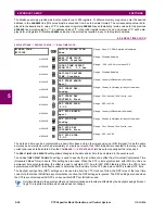
Page 587: ...upported in addition to the Highest DNP Levels Supported the complete list is described in the attached table Binary Inputs Object 1 Binary Input Changes Object 2 Binary Outputs Object 10 Control Relay Output Block Object 12 Binary Counters Object 20 Frozen Counters Object 21 Counter Change Event Object 22 Frozen Counter Event Object 23 Analog Inputs Object 30 Analog Input Changes Object 32 Analog...

Page 588: ...E Binary Outputs 4 Never Always Sometimes Configurable SELECT OPERATE Never 4 Always Sometimes Configurable DIRECT OPERATE Never 4 Always Sometimes Configurable DIRECT OPERATE NO ACK Never 4 Always Sometimes Configurable Count 1 4 Never Always Sometimes Configurable Pulse On Never Always 4 Sometimes Configurable Pulse Off Never Always 4 Sometimes Configurable Latch On Never Always 4 Sometimes Conf...

Page 589: ... 4 Configurable Only certain objects Sometimes attach explanation 4 ENABLE DISABLE unsolicited Function codes supported Sends Static Data in Unsolicited Responses 4 Never When Device Restarts When Status Flags Change No other options are permitted Default Counter Object Variation No Counters Reported Configurable attach explanation 4 Default Object 20 Default Variation 1 4 Point by point list atta...
Page 590: ...sol resp 17 28 index 3 Binary Input Change with Relative Time 1 read 06 no range or all 07 08 limited quantity 10 0 Binary Output Status Variation 0 is used to request default variation 1 read 00 01 start stop 06 no range or all 07 08 limited quantity 17 28 index 2 Binary Output Status 1 read 00 01 start stop 06 no range or all 07 08 limited quantity 17 28 index 129 response 00 01 start stop 17 28...

Page 591: ... Event Variation 0 is used to request default variation 1 read 06 no range or all 07 08 limited quantity 1 32 Bit Counter Change Event 1 read 06 no range or all 07 08 limited quantity 129 response 130 unsol resp 17 28 index 2 16 Bit Counter Change Event 1 read 06 no range or all 07 08 limited quantity 129 response 130 unsol resp 17 28 index 5 32 Bit Counter Change Event with Time 1 read 06 no rang...

Page 592: ... 129 response 130 unsol resp 17 28 index 3 32 Bit Analog Change Event with Time 1 read 06 no range or all 07 08 limited quantity 129 response 130 unsol resp 17 28 index 4 16 Bit Analog Change Event with Time 1 read 06 no range or all 07 08 limited quantity 129 response 130 unsol resp 17 28 index 5 short floating point Analog Change Event without Time 1 read 06 no range or all 07 08 limited quantit...

Page 593: ...atus 26 close 30 abort 5b free format 129 response 130 unsol resp 5b free format 5 File transfer 1 read 2 write 5b free format 129 response 130 unsol resp 5b free format 6 File transfer status 129 response 130 unsol resp 5b free format 7 File descriptor 28 get file info 5b free format 129 response 130 unsol resp 5b free format 80 1 Internal Indications 1 read 00 01 start stop index 7 129 response ...

Page 594: ...eze function is performed on a binary counter point the frozen value is available in the corresponding frozen counter point BINARY INPUT POINTS Static Steady State Object Number 1 Change Event Object Number 2 Request Function Codes supported 1 read 22 assign class Static Variation reported when variation 0 requested 2 Binary Input with status Configurable Change Event Variation reported when varia...

Page 595: ...14 14 Virtual Input 15 15 Virtual Input 16 16 Virtual Input 17 17 Virtual Input 18 18 Virtual Input 19 19 Virtual Input 20 20 Virtual Input 21 21 Virtual Input 22 22 Virtual Input 23 23 Virtual Input 24 24 Virtual Input 25 25 Virtual Input 26 26 Virtual Input 27 27 Virtual Input 28 28 Virtual Input 29 29 Virtual Input 30 30 Virtual Input 31 31 Virtual Input 32 32 Virtual Input 33 33 Virtual Input ...

Page 596: ...ear 10 freeze and clear noack 22 assign class Static Variation reported when variation 0 requested 1 32 Bit Binary Counter with Flag Change Event Variation reported when variation 0 requested 1 32 Bit Counter Change Event without time Change Event Buffer Size 10 Default Class for all points 3 FROZEN COUNTERS Static Steady State Object Number 21 Change Event Object Number 23 Request Function Codes ...

Page 597: ...adbands for all Analog Input points are in the same units as the Analog Input quantity For example an Analog Input quantity measured in volts has a corresponding deadband in units of volts This is in conformance with DNP Technical Bul letin 9809 001 Analog Input Reporting Deadband Relay settings are available to set default deadband values according to data type Deadbands for individual Analog Inp...

Page 598: ...E 12 C70 Capacitor Bank Protection and Control System GE Multilin E 2 DNP POINT LISTS APPENDIXE E ...

Page 599: ... C70 MANUAL REVISION U3 PAGE U2 PAGE U3 CHANGE DESCRIPTION Title Title Update Manual part number to 1601 9015 U3 2 18 2 18 Update Updated ENVIRONMENTAL specifications section 5 21 5 21 Update Updated IEC 61850 PROTOCOL section 5 145 5 145 Update Updated PHASE UNDERVOLTAGE section Table F 3 MAJOR UPDATES FOR C70 MANUAL REVISION U2 PAGE U1 PAGE U2 CHANGE DESCRIPTION Title Title Update Manual part nu...

Page 600: ...ANDS table 5 122 5 124 Update Updated PHASE INSTANTANEOUS OVERCURRENT section 5 129 5 131 Update Updated NEUTRAL DIRECTIONAL OVERCURRENT section 5 144 5 146 Update Updated PHASE OVERVOLTAGE section 5 155 5 157 Update Updated NEUTRAL VOLTAGE UNBALANCE section 5 169 5 170 Update Updated TIME OF DAY TIMERS section 5 180 5 182 Update Updated DIGITAL ELEMENTS section 5 186 5 188 Update Updated BREAKER ...

Page 601: ... TEST ERRORS section 7 9 7 10 Update Updated MINOR SELF TEST ERROR MESSAGES section B 8 B 8 Update Update MODBUS MEMORY MAP section Table F 7 MAJOR UPDATES FOR C70 MANUAL REVISION S2 PAGE S1 PAGE S2 CHANGE DESCRIPTION Title Title Update Manual part number to 1601 9015 S2 3 35 3 35 Update Updated MANAGED ETHERNET SWITCH OVERVIEW section 3 35 3 35 Update Updated MANAGED ETHERNET SWITCH MODULE HARDWA...

Page 602: ...section Table F 10 MAJOR UPDATES FOR C70 MANUAL REVISION R2 PAGE R1 PAGE R2 CHANGE DESCRIPTION Title Title Update Manual part number to 1601 9015 R2 Table F 11 MAJOR UPDATES FOR C70 MANUAL REVISION R1 Sheet 1 of 2 PAGE P2 PAGE R1 CHANGE DESCRIPTION Title Title Update Manual part number to 1601 9015 R1 2 3 2 3 Update Updated ORDERING section 2 5 2 5 Update Updated PROTECTION ELEMENTS specifications...

Page 603: ...RIPTION Title Title Update Manual part number to 1601 9015 P2 2 5 2 5 Update Updated PROTECTION ELEMENTS specifications section 2 9 2 9 Update Updated INPUTS specifications section 3 18 3 18 Update Updated CPU MODULE COMMUNICATIONS WIRING diagram to 842765A2 5 112 5 114 Update Updated NEUTRAL CURRENT UNBALANCE SCHEME LOGIC diagram to 834736A2 5 122 Add Added NEGATIVE SEQUENCE OVERVOLTAGE sub secti...

Page 604: ...ctor high set FDL Fault Detector low set FLA Full Load Current FO Fiber Optic FREQ Frequency FSK Frequency Shift Keying FTP File Transfer Protocol FxE FlexElement FWD Forward G Generator GE General Electric GND Ground GNTR Generator GOOSE General Object Oriented Substation Event GPS Global Positioning System HARM Harmonic Harmonics HCT High Current Time HGF High Impedance Ground Fault CT HIZ High ...

Page 605: ...mote Terminal Unit RX Rx Receive Receiver s second S Sensitive SAT CT Saturation SBO Select Before Operate SCADA Supervisory Control and Data Acquisition SEC Secondary SEL Select Selector Selection SENS Sensitive SEQ Sequence SIR Source Impedance Ratio SNTP Simple Network Time Protocol SRC Source SSB Single Side Band SSEL Session Selector STATS Statistics SUPN Supervision SUPV Supervise Supervisio...

Page 606: ...efective and it is returned with all transportation charges prepaid to an authorized service centre or the factory Repairs or replacement under war ranty will be made without charge Warranty shall not apply to any relay which has been subject to misuse negligence accident incorrect installation or use not in accordance with instructions nor any unit that has been altered outside a GE Multilin auth...

Page 607: ...5 72 5 73 FlexLogic operands 5 87 Modbus registers B 23 settings 5 70 BREAKER FAILURE description 5 107 determination 5 108 FlexLogic operands 5 87 logic 5 111 5 112 5 113 5 114 main path sequence 5 108 Modbus registers B 33 settings 5 106 5 109 specifications 2 11 BREAKER FLASHOVER FlexLogic operands 5 87 logic 5 191 Modbus registers B 12 settings 5 188 specifications 2 11 BREAKER RESTRIKE FlexLo...

Page 608: ...E B 6 DATE 7 6 DCMA INPUTS 6 19 Modbus registers B 15 B 30 settings 5 211 specifications 2 14 DCMA OUTPUTS description 3 21 Modbus registers B 36 settings 5 214 specifications 2 16 DEFINITE TIME CURVE 5 120 5 144 DESIGN 1 3 DEVICE ID 5 202 DEVICE PROFILE DOCUMENT E 1 DIELECTRIC STRENGTH 3 10 DIGITAL COUNTERS actual values 6 5 FlexLogic operands 5 88 logic 5 186 Modbus registers B 9 B 42 settings 5...

Page 609: ...FAST FORM C RELAY 2 15 FAST TRANSIENT TESTING 2 19 FAX NUMBERS 1 1 FEATURES 2 1 FIRMWARE REVISION 6 22 FIRMWARE UPGRADES 4 2 FLASH MESSAGES 5 12 FLEX STATE PARAMETERS actual values 6 6 Modbus registers B 14 B 34 settings 5 52 specifications 2 12 FLEXCURVES equation 5 120 Modbus registers B 23 B 42 settings 5 77 specifications 2 12 table 5 77 FLEXELEMENTS actual values 6 18 direction 5 102 FlexLogi...

Page 610: ... 37 IEEE CURVES 5 117 IMPORTANT CONCEPTS 1 4 IN SERVICE INDICATOR 1 17 7 8 INCOMPATIBLE HARDWARE ERROR 7 9 INPUTS AC current 2 14 5 65 AC voltage 2 14 5 66 contact inputs 2 14 5 196 5 218 dcmA inputs 2 14 3 21 direct inputs 2 14 IRIG B 2 14 3 26 remote inputs 2 14 5 202 5 203 5 204 RTD inputs 3 21 virtual 5 198 INSPECTION CHECKLIST 1 1 INSTALLATION communications 3 23 CT inputs 3 11 3 12 RS485 3 2...

Page 611: ... CURRENT UNBALANCE actual values 6 18 commands 7 5 FlexLogic operands 5 89 Modbus registers B 15 B 17 B 39 settings 5 135 specifications 2 10 theory of operation 9 12 NEUTRAL DIRECTIONAL OC Modbus registers B 30 NEUTRAL DIRECTIONAL OVERCURRENT FlexLogic operands 5 89 logic 5 135 polarization 5 133 settings 5 131 specifications 2 10 NEUTRAL INSTANTANEOUS OVERCURRENT see entry for NEUTRAL IOC NEUTRA...

Page 612: ...try for PHASE IOC PHASE IOC FlexLogic operands 5 90 logic 5 124 Modbus registers B 26 specifications 2 9 PHASE OVERVOLTAGE FlexLogic operands 5 90 logic 5 146 Modbus registers B 30 settings 5 146 specifications 2 11 PHASE ROTATION 5 67 PHASE TIME OVERCURRENT see entry for PHASE TOC PHASE TOC FlexLogic operands 5 90 logic 5 122 Modbus registers B 26 settings 5 121 specifications 2 9 PHASE UNDERVOLT...

Page 613: ...registers B 60 password protection 4 5 8 7 removing 4 7 8 9 viewing 4 6 8 8 SETTINGS CHANGING 4 26 SIGNAL SOURCES description 5 5 metering 6 12 settings 5 68 SIGNAL TYPES 1 3 SINGLE LINE DIAGRAM 2 1 2 2 SITE LIST CREATING 4 1 SNTP PROTOCOL error messages 7 11 Modbus registers B 20 settings 5 33 SOFTWARE installation 1 5 see entry for ENERVISTA UR SETUP SOFTWARE ARCHITECTURE 1 4 SOFTWARE PC see ent...

Page 614: ... PROGRAMMABLE LEDs custom labeling 4 21 defaults 4 16 description 4 15 4 16 Modbus registers B 21 settings 5 44 specifications 2 12 USER PROGRAMMABLE PUSHBUTTONS FlexLogic operands 5 93 Modbus registers B 24 B 32 settings 5 47 specifications 2 12 USER PROGRAMMABLE SELF TESTS Modbus registers B 22 settings 5 45 USERST 1 BIT PAIR 5 205 V VIBRATION TESTING 2 19 VIRTUAL INPUTS actual values 6 3 comman...

Reviews: