MB95630H Series
436
FUJITSU SEMICONDUCTOR LIMITED
MN702-00009-1v0-E
CHAPTER 21 MULTI-PULSE GENERATOR
21.6 Registers
21.6.4.1
16-bit MPG Output Data Buffer Register (Upper)
(OPDBRHx)
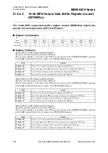
The 16-bit MPG output data buffer register (upper) (OPDBRHx) selects the pair
of OPDBRHx/OPDBRLx register whose data is to be loaded to the OPDUR/
OPDLR register, and the waveform to be loaded to the OPT5 pin and OPT4 pin.
■
Register Configuration
■
Register Functions
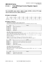
[bit7:4] BNKF, RDA[2:0]: OPDBRHx/OPDBRLx register select bits
These bits select data in which 16-bit MPG output data buffer register (upper/lower) (OPDBRHx/OPDBRLx)
is to be loaded to the OPDUR/OPDLR register. Data in the 16-bit MPG output data buffer register (upper/
lower) (OPDBRHx/OPDBRLx) selected is to be loaded to the OPDUR/OPDLR register.
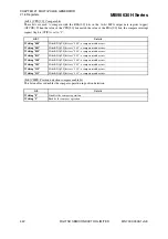
[bit3:2] OP5[1:0]: OPT5 output waveform select bits
These bits select the output waveform to the OPT5 pin.
The waveform selected is to be output to the OPT5 pin after the data in the OPDBRHx/OPDBRLx specified
in the BNKF bit and RDA[2:0] bits is loaded to the OPDUR/OPDLR register.
bit
7
6
5
4
3
2
1
0
Field
BNKF
RDA2
RDA1
RDA0
OP51
OP50
OP41
OP40
Attribute
R/W
R/W
R/W
R/W
R/W
R/W
R/W
R/W
Initial value
0
0
0
0
0
0
0
0
bit7:4
Details
Writing "0000"
Selects data in OPDBRH0/OPDBRL0 as the next data to be loaded to OPDUR/OPDLR.
Writing "0001"
Selects data in OPDBRH1/OPDBRL1 as the next data to be loaded to OPDUR/OPDLR.
Writing "0010"
Selects data in OPDBRH2/OPDBRL2 as the next data to be loaded to OPDUR/OPDLR.
Writing "0011"
Selects data in OPDBRH3/OPDBRL3 as the next data to be loaded to OPDUR/OPDLR.
Writing "0100"
Selects data in OPDBRH4/OPDBRL4 as the next data to be loaded to OPDUR/OPDLR.
Writing "0101"
Selects data in OPDBRH5/OPDBRL5 as the next data to be loaded to OPDUR/OPDLR.
Writing "0110"
Selects data in OPDBRH6/OPDBRL6 as the next data to be loaded to OPDUR/OPDLR.
Writing "0111"
Selects data in OPDBRH7/OPDBRL7 as the next data to be loaded to OPDUR/OPDLR.
Writing "1000"
Selects data in OPDBRH8/OPDBRL8 as the next data to be loaded to OPDUR/OPDLR.
Writing "1001"
Selects data in OPDBRH9/OPDBRL9 as the next data to be loaded to OPDUR/OPDLR.
Writing "1010"
Selects data in OPDBRHA/OPDBRLA as the next data to be loaded to OPDUR/OPDLR.
Writing "1011"
Selects data in OPDBRHB/OPDBRLB as the next data to be loaded to OPDUR/OPDLR.
Writing a value
other those above
Setting prohibited
bit3:2
Details
Writing "00"
Selects "L" level as the waveform to be output to the OPT5 pin.
Writing "01"
Selects the output of the PPG timer as the waveform to be output to the OPT5 pin.
Writing "10"
Selects the inverted output as the waveform to be output to the OPT5 pin.
Writing "11"
Selects "H" level as the waveform to be output to the OPT5 pin.


