


Enhanced Modular Input/Output Subsystem (eMIOS200)
23-56
Freescale Semiconductor
PXR40 Microcontroller Reference Manual, Rev. 1
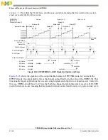
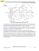
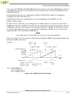
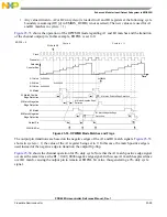
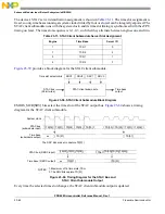
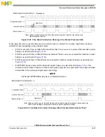
Figure 23-50. OPWMCB with 100% Duty Cycle (A1 = 4 and B1 = 3)
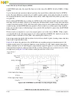
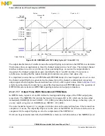
The output disable feature, if enabled, causes the output flip-flop to transition to the EDPOL inverted state.
This feature allows an application to force the channel output pin to a “safe” state. The internal channel
matches continue to occur even in this case, thus generating flags. As soon as the output disable is
deasserted, the channel output pin is again controlled by the A1 and B1 matches. This process is
synchronous, meaning that the output channel pin transitions on system clock edges only.
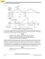
It is important to notice that, as in OPWMB and OPWFMB modes, the match signal used to set or clear
the channel output flip-flop is generated on the deassertion of the channel combinational comparator
output signal, which compares the selected time base with A1 or B1 register values. Refer to
which shows the delay from matches to output flip-flop transition in OPWFMB mode. The operation of
OPWMCB mode is similar to OPWFMB regarding matches and output pin transition.
23.4.1.1.17
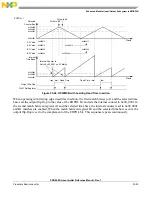
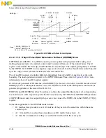
Output Pulse Width Modulation (OPWM) Mode
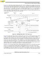
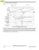
In OPWM mode, registers A1 and B1 define the leading and trailing edges of the PWM output pulse,
respectively. The MODE[6] bit controls the transfer from register B2 to B1, which can be done either
immediately (MODE[6] cleared, MODE = 010_00b0), providing the fastest change in the duty cycle, or
at every match of register A1 (MODE[6] set, MODE = 010_00b1).
The value loaded in register A1 is compared with the value on the selected time base. When a match on
comparator A occurs, the output flip-flop is set to the value of the EDPOL bit. When a match occurs on
comparator B, the output flip-flop is set to the complement of the EDPOL bit.
FLAG can be generated at match B, when MODE[5] is cleared, or in both matches, when MODE[5] is set.
0x000001
0x000020
0x000004
A1 Value
A2 Value
B1 Value
B2 Value
0x000004
0x000001
Output Flip-Flop
0x000003
0x000015
0x000003
0x000015
0x000003
Selected
Counter Bus
Time
Write to B2
Time
Cycle n
Cycle (n + 1)
Cycle (n + 2)
Dead Time
Dead Time
Dead Time
Internal Time Base
Summary of Contents for PXR4030
Page 1: ...PXR40 Microcontroller Reference Manual Devices Supported PXR4030 PXR4040 PXR40RM Rev 1 06 2011...
Page 30: ...PXR40 Microcontroller Reference Manual Rev 1 Freescale Semiconductor xxx...
Page 40: ...PXR40 Microcontroller Reference Manual Rev 1 xl Freescale Semiconductor...
Page 66: ...Memory Map PXR40 Microcontroller Reference Manual Rev 1 2 4 Freescale Semiconductor...
Page 120: ...Signal Descriptions 3 54 Freescale Semiconductor PXR40 Microcontroller Reference Manual Rev 1...
Page 860: ...FlexCAN Module 24 50 Freescale Semiconductor PXR40 Microcontroller Reference Manual Rev 1...
Page 1167: ...Decimation Filter Freescale Semiconductor 28 53 PXR40 Microcontroller Reference Manual Rev 1...
Page 1168: ...Decimation Filter 28 54 Freescale Semiconductor PXR40 Microcontroller Reference Manual Rev 1...


