


Signal Descriptions
Freescale Semiconductor
3-51
PXR40 Microcontroller Reference Manual, Rev. 1
3.3.10
Reset and Clock Signals
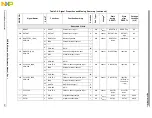
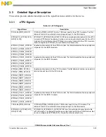
D_RD_WR_GPIO294
Indicates whether an external bus transfer is a read or write operation.
D_WE0_GPIO295
Write/Byte enable specify which data pins contain valid data for an external bus transfer.
D_WE1_GPIO296
D_OE_GPIO297
Output enable indicates that the EBI is ready to accept read data.
D_TS_GPIO298
Transfer start is asserted by the EBI owner to indicate the start of a transfer.
D_ALE_GPIO299
Address latch enable is used to demultiplex the address from data bus. It is asserted while
the least significant 16 bits of the address are present in the multiplexed address/data bus.
D_TA_GPIO300
Transfer acknowledge is asserted by the EBI owner to acknowledge that the slave has
completed the current transfer.
D_CS1_GPIO301
EBI chip select output signal.
D_BDIP_GPIO302
Burst Data In Progress indicates that an EBI burst transfer is in progress.
D_WE2_GPIO303
Write/Byte enable specify which data pins contain valid data for an external bus transfer.
D_WE3_GPIO304
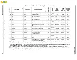
D_ADD9_GPIO305
EBI address signals.
D_ADD10_GPIO306
D_ADD11_GPIO307
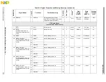
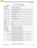
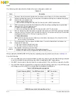
Table 3-14. Reset and Clock Signals
Signal Name
Description
RESET
The RESET input is asserted by an external device to reset the all modules of the device
MCU. The RESET pin must be asserted during a power-on reset.
RSTOUT
The RSTOUT output is a push/pull output that is asserted during an internal device reset.
The pin can also be asserted by software without causing an internal reset of the device
MCU.
Note: During a power-on-reset (POR), RSTOUT is tri-stated.
BOOTCFG[0:1]_IRQ[2:3]_
GPIO[211:212]
BOOTCFG[0:1] signals are sampled on every reset. The values are used by the Boot
Assist Module (BAM) program to determine the boot configuration of the device. The
alternate functions are the external interrupt request inputs (IRQs).
WKPCFG_NMI_GPIO213
WKPCFG (sampled at every reset) determines whether specific eTPU and eMIOS pins
are connected to a weak pullup or weak pulldown during and immediately after reset. The
alternate function (NMI) is a critical interrupt to the core.
PLLCFG0_IRQ4_GPIO208
PLLCFGn are sampled at every reset. These values are used to configure the FMPLL
mode of operation. The alternate function is an external interrupt request input.
PLLCFG1_IRQ5_GPIO209
PLLCFGn are sampled at every reset. These values are used to configure the FMPLL
operation mode. The alternate functions are an external interrupt request input and data
output for the DSPI module D.
PLLCFG2
PLLCFGn are sampled at every reset. These values are used to configure the FMPLL
operation mode. PLLCFG2 configures the crystal oscillator range.
Table 3-13. EBI Signals (Development Bus Only) (continued)
Signal Name
Description
Summary of Contents for PXR4030
Page 1: ...PXR40 Microcontroller Reference Manual Devices Supported PXR4030 PXR4040 PXR40RM Rev 1 06 2011...
Page 30: ...PXR40 Microcontroller Reference Manual Rev 1 Freescale Semiconductor xxx...
Page 40: ...PXR40 Microcontroller Reference Manual Rev 1 xl Freescale Semiconductor...
Page 66: ...Memory Map PXR40 Microcontroller Reference Manual Rev 1 2 4 Freescale Semiconductor...
Page 120: ...Signal Descriptions 3 54 Freescale Semiconductor PXR40 Microcontroller Reference Manual Rev 1...
Page 860: ...FlexCAN Module 24 50 Freescale Semiconductor PXR40 Microcontroller Reference Manual Rev 1...
Page 1167: ...Decimation Filter Freescale Semiconductor 28 53 PXR40 Microcontroller Reference Manual Rev 1...
Page 1168: ...Decimation Filter 28 54 Freescale Semiconductor PXR40 Microcontroller Reference Manual Rev 1...


