


MPC563XM Reference Manual, Rev. 1
Freescale Semiconductor
405
Preliminary—Subject to Change Without Notice
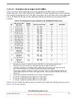
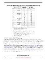
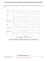
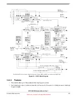
Figure 13-58. Address/Data Multiplexing with a 32-bit bus
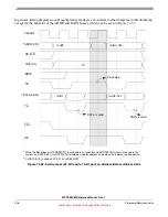
CLKOUT
CS0
**ADDR[3:31]/DATA[0:31]
TS
WE0/BE0
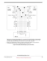
MCU
EXTAL
ADDR[3:31]/DATA[0:31]
CS0
TS
BDIP
BDIP
BR
BG
BB
TA
TEA
BR
BG
BB
TA
TEA
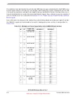
MCU
Memory
CK
CS
AD
V
WE
*A/D[31:0]
BAA
TSIZ[0:1]
RD_WR
RD_WR
WE0/BE0
* Most memories have the LSB signified by bit 0, this must match the LSB of the MCU, signified by bit 31.
TSIZ[0:1]
(configured
for internal
arbitration)
(configured
for external
arbitration)
If the memory is word addressable, other bits of the data bus can be used. For example, a 32-bit Flash
might need A[2] as the LSB, where A/D1 & A/D0 are not used for address decoding.
OE
OE
OE
** These refer to the DATA pins of the MCU, which are used for both address and data functions
in this system. Note that a few of the upper DATA pins are data-only.


