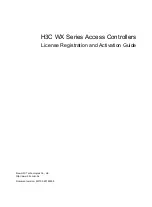
44.4.4.2 Classic SPI Transfer Format (CPHA = 1)
This transfer format shown in the following figure is used to communicate with
peripheral SPI slave devices that require the first SCK edge before the first data bit
becomes available on the slave SOUT pin. In this format, the master and slave devices
change the data on their SOUT pins on the odd-numbered SCK edges and sample the
data on their SIN pins on the even-numbered SCK edges.
t
ASC
= After SCK delay
t
CSC
=
PCS to SCK delay
MSB first (LSBFE = 0): MSB
t
DT
=
Delay after Transfer (minimum CS negation time)
t
CSC
Bit 1
MSB
t
DT
tASC
PCSx/SS
Slave SOUT
Master SIN/
Master SOUT/
Slave SIN
Master and Slave
Sample
SCK (CPOL = 0)
1
2
3
4
5
6
7
8
9 10 11 12 13 14 15 16
SCK (CPOL = 1)
Bit 6
Bit 2
Bit 3
Bit 4
Bit 5
Bit 6
LSB
Bit 5
Bit 4
Bit 3
Bit 2
Bit 1
LSB first (LSBFE = 1): LSB
Figure 44-73. Module transfer timing diagram (MTFE=0, CPHA=1, FMSZ=8)
The master initiates the transfer by asserting the PCS signal to the slave. After the t
CSC
delay has elapsed, the master generates the first SCK edge and at the same time places
valid data on the master SOUT pin. The slave responds to the first SCK edge by placing
its first data bit on its slave SOUT pin.
At the second edge of the SCK the master and slave sample their SIN pins. For the rest of
the frame the master and the slave change the data on their SOUT pins on the odd-
numbered clock edges and sample their SIN pins on the even-numbered clock edges.
After the last clock edge occurs, a delay of t
ASC
is inserted before the master negates the
PCS signal. A delay of t
DT
is inserted before a new frame transfer can be initiated by the
master.
Functional description
K22F Sub-Family Reference Manual , Rev. 3, 7/2014
1080
Freescale Semiconductor, Inc.