


Errata for Revision 1.0
MCF5282 User’s Manual Errata, Rev. 15
Freescale Semiconductor
7
4
Errata for Revision 1.0
Table 4. MCF5282UM Rev 1.0 Errata
Location
Description
1.1/1-1
Change ‘Real time debug support, with two user-visible hardware breakpoint registers’
To ‘Real time debug support, with one user-visible hardware breakpoint register’
Table 2-2/2-7
Change the I field description to read: “Interrupt level mask. Defines the current interrupt
level. Interrupt requests are inhibited for all priority levels less than or equal to the current
level, except the edge-sensitive level 7 request, which cannot be masked.”
Table 5-1/5-2
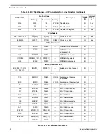
Replace the description of PRI1 and PRI2 with the following:
Table 5-1/5-3
Add the following note to the SPV bit description: “The BDE bit in the second RAMBAR
register must also be set to allow dual port access to the SRAM. For more information,
see Section 8.4.2, ‘Memory Base Address Register (RAMBAR).’”
Description
Priority bit. PRI1 determines if DMA or CPU has priority in upper 32K bank of
memory. PRI2 determines if DMA or CPU has priority in lower 32K bank of
memory. If bit is set, DMA has priority. If bit is reset, CPU has priority. Priority is
determined according to the following table.
NOTE: The Motorola-recommended setting for the priority bits is 00.
PRI[1:2]
Upper Bank
Priority
Lower Bank
Priority
00
DMA Accesses
DMA Accesses
01
DMA Accesses
CPU Accesses
10
CPU Accesses
DMA Accesses
11
CPU Accesses
CPU Accesses


