


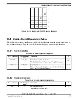


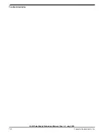

1
A
PTA12
B
PTB3
C
PTA9
D
PTA8
1
E
PTA7
2
PTB13
PTB5
PTB4
PTB2
2
PTB0
3
PTA0
PTA2
VREFL
VSS
PTB1
3
PTA5
4
PTA1
VDD
VREFH
PTA3
PTA4
4
PTA6
A
B
C
D
E
Figure 10-2. KL02 20-pin WLCSP pinout diagram
10.4 Module Signal Description Tables
The following sections correlate the chip-level signal name with the signal name used in
the module's chapter. They also briefly describe the signal function and direction.
10.4.1 Core modules
Table 10-3. SWD signal descriptions
Chip signal name
Module signal
name
Description
I/O
SWD_DIO
SWD_DIO
Serial Wire Debug Data Input/Output
The SWD_DIO pin is used by an external debug tool for
communication and device control. This pin is pulled up internally.
Input /
Output
SWD_CLK
SWD_CLK
Serial Wire Clock
This pin is the clock for debug logic when in the Serial Wire Debug
mode. This pin is pulled down internally.
Input
10.4.2 System modules
Table 10-4. System signal descriptions
Chip signal name
Module signal
name
Description
I/O
NMI_b
—
Non-maskable interrupt
I
Table continues on the next page...
Chapter 10 Signal Multiplexing and Signal Descriptions
KL02 Sub-Family Reference Manual, Rev. 2.1, July 2013
Freescale Semiconductor, Inc.
127


