


fication of 1x10
-10
per 24h is reached only after 48h of contin-
uous operation.
– The frequency uncertainty for standard oscillators is
mainly dependent on the ambient temperature. Variations
in ambient temperature between 0
°
C and +50
°
C may
cause a frequency change of up to 100 Hz, whereas the
aging per month is only 5 Hz. During warm-up the tem-
perature increase inside the counter will affect the oscil-
lator for about two hours.
n
How often should you calibrate?
In the table on the preceding page you can see the uncertainty
of your time base oscillator for various MTBRC (Mean Time
Between Recalibration) intervals.
Compare the requirements of your application with the values
in the table, and select the proper MTBRC accordingly.
Please note that the frequency uncertainty when operating in a
temperature controlled environment is different from field
use. See the two sections in the table.
+
When adjusted, keep in mind that the reference
crystal oscillator will be compensated only for fre-
quency deviation caused by aging.
Timebase Calibration Procedure
n
Test Equipment
The instrumentation outlined here is an example of equipment
meeting the minimum requirements for calibrating the differ-
ent timebase options. You are free to choose other equipment
as long as its performance is adequate for the purpose.
A suitable reference oscillator can be derived from a number
of sources, the specifications of which determine the type of
DUT timebase option that can be calibrated.
The table suggests a number of possible combinations. Re-
member this rule of thumb: the reference should be at least
five times better than the DUT for a reliable calibration result.
n
Work Instructions
– Determine the minimum requirements of the reference
oscillator and make a signal meeting these requirements
available at your test site.
NOTE:
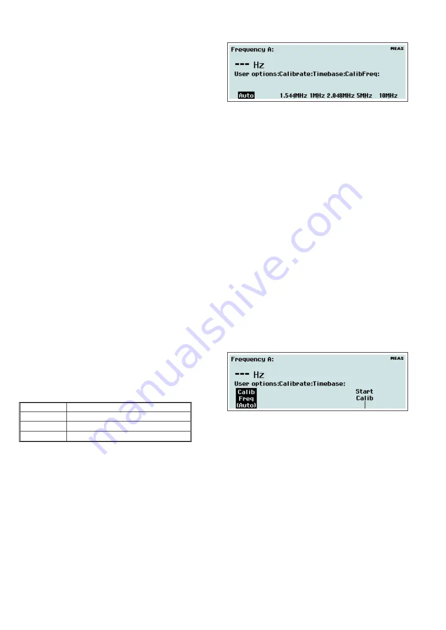
You can use a number of different calibration fre-
quencies for the DUT: 1 MHz, 1.544 MHz, 2.048 MHz,
5 MHz and 10 MHz.
– Place the DUT in its calibration environment, preferably
at an ambient temperature of +23 ± 2 °C and power it
up.
– Recall the default settings by keying in the following se-
quence:
USER OPT
®
Save/Recall
®
Recall Setup
®
Default
– Let the DUT assume its final internal operating tempera-
ture. Allow at least a warm-up period of two hours be-
fore proceeding.
– Connect the reference oscillator signal to Input A on the
DUT.
– Select 10 s measuring time (under
SETTINGS
) and mea-
sure the frequency.
NOTE:
Use a measuring time that is long enough to meet the
required resolution (see Table 7-1) or use statistics to
find the mean value of multiple measurements.
– Calculate the relative deviation of the internal timebase
as
D
rel
= -(f
meas
- f
ref
)/f
ref
.
– Translate this value to an absolute deviation
D
abs
of the
internal 10 MHz timebase by using the expression:
D
abs
=
D
rel
´
10
7
(Hz)
– Note this value as the calibration state before adjust-
ment, and decide if an adjustment is necessary according
to the applicable criteria.
– Stop here if an adjustment is not necessary. Otherwise
go on.
– Go to the
Calibration Submenu
and select
Timebase
.
– Press
Calib Freq
and select one of the possible frequen-
cies, or let the counter decide on its own by accepting
the preselected
Auto
setting.
– Start the calibration procedure by pressing
Start Calib
and follow the instructions on the display.
– You must enter a date at the end of the procedure in or-
der to make the result the active user calibration.
– Measure the external reference frequency once more,
and calculate the deviation of the internal timebase in
the same way as before the adjustment. Note this value
as the calibration state after adjustment.
– Compare the two deviation values, and check that the
calibration procedure has been successful.
– Fill out the calibration protocol if required.
7-4
Frequency Reference
DUT Option
Reference Oscillator
Standard
PM6690/_5_
PM6690/_5_
909
PM6690/_6_
909
Table 7-2
Reference Oscillator requirements.
Summary of Contents for PM6690
Page 1: ...Timer Counter Analyzer PM6690 Service Manual...
Page 4: ...This page is intentionally left blank IV...
Page 7: ...Chapter 1 Safety Instructions...
Page 11: ...Chapter 2 Performance Check...
Page 18: ...This page is intentionally left blank 2 8 Performance Check RF Options...
Page 19: ...Chapter 3 Disassembly...
Page 23: ...Chapter 4 Circuit Descriptions...
Page 24: ...This page is intentionally left blank 4 2...
Page 41: ...Chapter 5 Corrective Preventive Maintenance...
Page 44: ...This page is intentionally left blank 5 4 Other Important Information...
Page 45: ...Chapter 6 Repair...
Page 46: ...This page is intentionally left blank 6 2...
Page 104: ...This page is intentionally left blank 6 60 Safety Inspection and Test After Repair...
Page 105: ...Chapter 7 Calibration Adjustments...
Page 119: ...Chapter 8 Replacement Parts...
Page 147: ...Chapter 9 Schematic Diagrams...
Page 150: ...This page is intentionally left blank 9 4 Schematic Diagrams...
Page 151: ...This page is intentionally left blank Schematic Diagrams 9 5...
Page 152: ...Main Board PCB 1 Component Layout 9 6 Schematic Diagrams...
Page 154: ...9 8 Schematic Diagrams This page is intentionally left blank...
Page 156: ...9 10 Schematic Diagrams This page is intentionally left blank...
Page 158: ...9 12 Schematic Diagrams This page is intentionally left blank...
Page 160: ...9 14 Schematic Diagrams This page is intentionally left blank...
Page 162: ...9 16 Schematic Diagrams This page is intentionally left blank...
Page 164: ...9 18 Schematic Diagrams This page is intentionally left blank...
Page 166: ...This page is intentionally left blank 9 20 Schematic Diagrams...
Page 168: ...Display Keyboard PCB 2 Component Layout 9 22 Schematic Diagrams...
Page 170: ...This page is intentionally left blank 9 24 Schematic Diagrams...
Page 172: ...This page is intentionally left blank 9 26 Schematic Diagrams...
Page 173: ...Main Board PCB 1 Component Layout Bottom Side Schematic Diagrams 9 27...
Page 174: ...Main Board PCB 1 Component Layout Top Side 9 28 Schematic Diagrams...
Page 176: ...9 30 Schematic Diagrams This page is intentionally left blank...
Page 178: ...9 32 Schematic Diagrams This page is intentionally left blank...
Page 180: ...9 34 Schematic Diagrams This page is intentionally left blank...
Page 182: ...9 36 Schematic Diagrams This page is intentionally left blank...
Page 184: ...9 38 Schematic Diagrams This page is intentionally left blank...
Page 186: ...9 40 Schematic Diagrams This page is intentionally left blank...
Page 188: ...9 42 Schematic Diagrams This page is intentionally left blank...
Page 190: ...Display Keyboard PCB 2 Component Layout 9 44 Schematic Diagrams...
Page 192: ...9 46 Schematic Diagrams This page is intentionally left blank...
Page 193: ...Chapter 10 Appendix...
Page 196: ...This page is intentionally left blank 10 4 Glossary...
Page 197: ...Chapter 11 Index...
Page 200: ...This page is intentionally left blank 11 4 Index...