


9100A-017
7-14
gate whose output is connected to WAIT. If either signal
goes low, the WAIT input will go low as well. For trou-
bleshooting in the case of no DTACK, both the VDTACK
and VWAIT lines should also be connected to Vector
Output I/O Module pins where their activity can be moni-
tored.
•
+5V, GND
An external power supply provides the required voltages to
a DPDT switch that controls power to the video board.
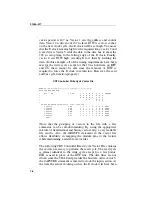
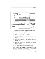
Determining Bus Cycles
7.14.
The SCN2674 Advanced Video Display Controller timing dia-
grams and the video board schematic (found in the 9100 Series
Service Manual) can be used to determine the vector patterns
necessary to perform bus cycles (see Figure 7-2). Signals PS7
and PS6 are formed by address strobe AS and memory decoding
(PS7 = $FXXXX, PS6 = $EXXXX) on the 9100A main board.
To access either the controller or video RAM requires the same
basic cycle, the only difference being the controller data is D7
through D0 and is selected by PS7, while the video RAM data is
D15 through D0 and is selected by PS6.
Because of the similarity of the cycles to access the controller
and the video RAM, only the bus cycles to the controller are
illustrated in this section.
The video input PS7 provides CE and also exits the board as
VDTACK. The R/W signal is “ANDed” with LDS to get the RD
and WR signals.
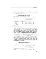
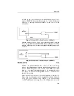
Determining the Write Cycle
7.15.
Examine the SCN2674 4 MHz write cycle timing diagram to
learn how its signals interface with the video board. To perform
a write cycle, the following events must occur:
•
Address bus A11 through A1 must be set a minimum of 30
ns prior to WR going low (R/W low and LDS low).
Summary of Contents for 9100A Series
Page 6: ...vi ...
Page 8: ...viii ...
Page 10: ...x ...
Page 14: ...9100A 017 1 4 ...
Page 24: ...9100A 017 3 6 ...
Page 44: ...9100A 017 5 4 ...
Page 58: ...9100A 017 6 14 ...
Page 83: ...A 1 Appendix A New TL 1 Commands ...
Page 84: ...9100A 017 A 2 ...
Page 87: ...clockfreq 3 For More Information The Overview Of TL 1 section of the Programmer s Manual ...
Page 88: ...clockfreq 4 ...
Page 91: ...drivepoll 3 For More Information The Overview Of TL 1 section of the Programmer s Manual ...
Page 92: ...drivepoll 4 ...
Page 104: ...vectordrive 4 ...
Page 107: ...vectorload 3 For More Information The Overview Of TL 1 section of the Programmer s Manual ...
Page 108: ...vectorload 4 ...
Page 116: ...9100A 017 C 2 ...
Page 117: ...9100A 017 C 3 ...
Page 118: ...9100A 017 C 4 ...


