


9100A-017
7-10
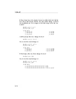
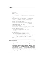
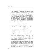
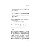
2 $B8000 $41 1 1 0 1 0 0 X X XXXX
WAIT +
3 $B8000 $XX 1 1 1 1 0 0 X X XXXX
STOP
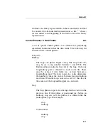
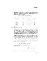
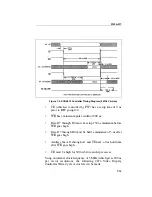
In the Video RAM Read Cycle Vector File that follows, vector 1
sets addresses A19 through A0 and data D7 through D0 to tri-
state. Vector 2 holds the address and data while MEMR goes
low. Upon receipt of MEMR and the correct address, IORDY
goes low. The module then waits until the UUT acknowledges
the read (by returning the IORDY line high), which satisfies the
WAIT condition. Vector driving then continues. Vector 3
maintains the address and MEMR while the CAPTURE Clock
clocks the data on the bus. Vector 4 returns MEMR high to fin-
ish up the cycle.
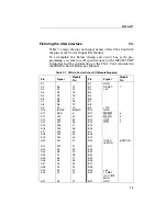
Video RAM Read Cycle Vector File
GROUPS [40-21][20-13][1][2][3][4][5][7][8][6][12-9]
DISPLAY HEX,HEX,BIN
! A19 - A0 D7-D0 I I M M A R I I UNUSED
! O O E E E E O O
! R W M M N S R C
! - - W R E D L
! - - T Y K
!
! READ CYCLE address $B8000
1 $B8000 $XX 1 1 1 1 0 0 X X XXXX
2 $B8000 $XX 1 1 1 0 0 0 X X XXXX
WAIT +
3 $B8000 $XX 1 1 1 0 0 0 X X XXXX
CAPTURE
4 $B8000 $XX 1 1 1 1 0 0 X X XXXX
STOP
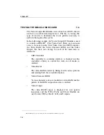
Vector File Generation
7.9.
Once the basic read and write cycles have been determined, the
vector files to control and test the CGA Card can be built. One
vector file can contain the initialization routines for the CGA
Card for the 40 Column, 80 Column, and Graphics Modes. This
consists of a sequence of writes to the CRT Controller. The data
required for each register is described in the 6845 Register
Description in the Color/ Graphics Monitor Adapter Section in
the IBM Technical Reference Manual.
Other vector files can be built to read and write to various
registers for testing the CRT Controller, and to write various
patterns into video RAM and to read back the values. In
Summary of Contents for 9100A Series
Page 6: ...vi ...
Page 8: ...viii ...
Page 10: ...x ...
Page 14: ...9100A 017 1 4 ...
Page 24: ...9100A 017 3 6 ...
Page 44: ...9100A 017 5 4 ...
Page 58: ...9100A 017 6 14 ...
Page 83: ...A 1 Appendix A New TL 1 Commands ...
Page 84: ...9100A 017 A 2 ...
Page 87: ...clockfreq 3 For More Information The Overview Of TL 1 section of the Programmer s Manual ...
Page 88: ...clockfreq 4 ...
Page 91: ...drivepoll 3 For More Information The Overview Of TL 1 section of the Programmer s Manual ...
Page 92: ...drivepoll 4 ...
Page 104: ...vectordrive 4 ...
Page 107: ...vectorload 3 For More Information The Overview Of TL 1 section of the Programmer s Manual ...
Page 108: ...vectorload 4 ...
Page 116: ...9100A 017 C 2 ...
Page 117: ...9100A 017 C 3 ...
Page 118: ...9100A 017 C 4 ...


