background image

7-1

Section 7

Applications

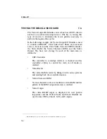
USING THE VECTOR OUTPUT I/O MODULE

7.1.

The Vector Output I/O Module can be used in a wide variety of
applications, from simple pattern stimulus to performing bus
cycles such as read and write cycles. Regardless of the
application, five main steps are required to fully use the
capabilities of the module. These are:

1.

Create the vector files using the editor or another source.

2.

From TL/1, use a program to setup the output section.

3.

From TL/1, use a program to setup the input section.

4.

From TL/1, use a program to drive vectors and measure
responses.

5.

From TL/1, use a program to process the results.

Section 6 “Using the Vector Editor” illustrated how to make
vector files. (To make vector files that perform bus cycles, see
“Bus Emulation”, “Testing the IBM CGA Video Card”, and
“68000 Bus Video Application” further on in this section.)

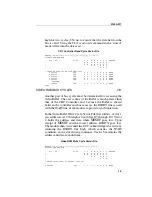
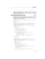
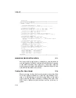
The following example shows a typical program with the four
steps necessary for setting up the output and input sections,
driving vectors and measuring responses, and processing the
results.

Summary of Contents for 9100A Series

Page 1: ...9100A Series 9100A 017 Vector Output I O Module P N 855437 May 1989 1989 John Fluke Mfg Co Inc All rights reserved Litho in U S A ...

Page 2: ...btain warranty service contact a Fluke Service Center or send the product with the description of the difficulty postage prepaid to the nearest Fluke Service Center Fluke assumes no risk for damage in transit Fluke will at our option repair or replace the defective product free of charge However if we determine that the failure was caused by misuse alteration or abnormal condition of operation or ...

Page 3: ...utput Operation 3 1 3 1 INTRODUCTlON 3 1 3 2 CLOCK SELECTION 3 1 3 3 VECTOR LOADING 3 2 3 4 VECTOR DRIVING 3 2 3 5 LOOP CONTROL 3 2 3 6 HANDSHAKING 3 2 3 7 STOPPING VECTOR DRIVING 3 3 3 8 TRISTATE CONTROL 3 4 3 9 COMPLETION STATUS 3 5 4 Hardware 4 1 4 1 PHYSICAL DESCRIPTION 4 1 4 2 CONNECTING THE MODULE TO THE MAINFRAME 4 5 4 3 PERFORMING THE MODULE SELF TEST 4 6 4 4 CALIBRATING THE MODULE 4 6 4 5...

Page 4: ...MODULE VECTORS 4 16 5 TL 1 Functions 5 1 5 1 INTRODUCTION 5 1 5 2 CLOCKFREQ 5 1 5 3 DRIVEPOLL 5 1 5 4 EDGEOUTPUT 5 2 5 5 ENABLEOUTPUT 5 3 5 6 STROBEOUTCLOCK 5 3 5 7 SYNCOUTPUT 5 3 5 8 VECTORDRIVE 5 3 5 9 VECTORLOAD 5 3 6 Using the Vector Editor 6 1 6 1 INTRODUCTION 6 1 6 2 CREATING A NEW VECTOR FILE 6 1 6 3 SOFTKEY OPERATIONS 6 2 6 4 WORKING WITH THE VECTOR FILE 6 4 6 5 The Groups Line 6 4 6 6 The...

Page 5: ...xample 7 11 7 11 68000 BUS VIDEO APPLICATION 7 12 7 12 Testing The Video Board 7 12 7 13 Fixturing the Video Board Interface 7 13 7 14 Determining Bus Cycles 7 14 7 15 Determining the Write Cycle 7 14 7 16 Determining the Read Cycle 7 16 7 17 WAIT APPLICATION 7 18 7 18 TIMING SETS 7 19 7 19 TL 1 VECTOR FILE GENERATION 7 21 Appendices A New TL 1 Commands A 1 B I O Module Clip Pin Mapping B 1 C Keyp...

Page 6: ...vi ...

Page 7: ...vii Tables Table Title Page 2 1 Vector Output I O Module Specifications 2 1 7 1 CGA to Vector Output I O Module Mapping 7 5 7 2 Video Board to Vector Output I O Module Mapping 7 13 ...

Page 8: ...viii ...

Page 9: ...ion 4 4 4 3 Input Section Block Diagram 4 5 4 4 Pod Sync Input Output Section Timing Diagram 4 13 4 5 Capture Clock Timing Diagram 4 15 5 1 Vector I O Control 5 2 7 1 MC6845 Cycle Timing Diagram 7 7 7 2 SCN2674 Controller Timing Diagram 7 15 7 3 Using WAIT to Check for a Level Method 1 7 19 7 4 Using WAIT to Check for a Level Method 2 7 19 7 5 Connecting Two Modules for Timing Sets 7 20 ...

Page 10: ...x ...

Page 11: ...ctor Output I O Module allows you to drive vectors parallel patterns with four different clock modes Vectors can be clocked out at up to 25 MHz using an external clock source Each 40 pin module also provides a selectable internal clock generator of 1 5 10 or 20 MHz The clock can be qualified by external lines that control start stop and enable A handshaking line allows additional synchronization b...

Page 12: ...n of the test vector patterns can be accomplished in two ways using the 9100A Editor or downloading from another system The 9100A Editor has been enhanced to effectively enter test vectors for the 9100A 017 Vectors can be entered in user pro grammable groups in hexadecimal notation binary notation or a mixture of both The vector editor displays the vector information in the order set by the pin gr...

Page 13: ...ted by the vector file To create a vector file using the 9100A Editor you need to edit a file of the new type VECTOR which has been added under each UUT directory The file type should be specified as VECTOR when editing the file Eight new TL 1 built in functions have been added to the 9100A Test Language TL 1 to support the new Vector Output I O Module These functions are Clockfreq Drivepoll Edgeo...

Page 14: ...9100A 017 1 4 ...

Page 15: ...ansition times clocks 5 ns all others 12 ns Table 2 1 Vector Output I O Module Specifications VECTOR OUTPUT I O MODULE OUTPUT SECTION into 10 LS TTL loads with card edge connector attached Module Vector Size 8192 Vectors 40 Channels Wide Maximum Vector Pattern 4 Modules 8192 Vectors 160 Channels Wide Vector Looping Up to 65536 Repetitions of One Vector Set Output Logic Levels High 3 7V minimum 6 0...

Page 16: ...R CLK for the vector to be output by that dock otherwise that vector is only driven internally and the output is held tri stated effectively skipping that vector Output Series Termination 33 Ohms Capture Clock INT CLK Capture Clock clocks 42 5 ns 5 ns after the falling edge of INT CLK DR CLK Capture Clock clocks 55 ns 10 ns after non clocking edge of DR CLK approximate 50 duty cycle START STOP and...

Page 17: ...z minimum Maximum Count Transition Mode 8388608 23 bits counts overflow Frequency Accuracy Frequency Mode 250 ppm 2 Hz Stop Counter Maximum Frequency 10 MHz Maximum Count 65535 clocks Clock Maximum Frequency 10 MHz Minimum Pulse Width 50ns Timing for Synchronous Measurements Maximum Frequency of Clock 10 MHz Maximum Frequency of Data 5MHz Data Setup Time 30 ns minimum Data Hold Time 30 ns minimum ...

Page 18: ...edge for clock edge to be recognized 10 ns minimum Data Timing for Asynchronous Measurements Maximum Frequency 10 MHz Minimum Pulse Width HIGH or LOW 50 ns Minimum Pulse Width tri state 150 ns Data Compare Equal Minimum Pulse Width of Data and Enable 75ns PHYSICAL SPECIFICATIONS Operating Temperature 5 to 27 C 95 RH maximum non condensing 27 to 40 C RH decreasing linearly form 95 to 50 non condens...

Page 19: ...ule can be connected to a UUT clock source The syncoutput command would then be set to drclk To synchronize re sponse gathering with a UUT clock connect the Vector Output I O Module CLOCK input yellow lead to the UUT clock source and set the sync command to ext To synchronize the UUT to the Vector Output I O Module con nect the UUT clock input to INT CLK and set the syncoutput command to intfreq U...

Page 20: ...e and clock signals In the second mode of operation driving begins after the execution of the TL 1 arm command and upon the receipt of the proper start enable and clock signals The second mode permits the simultaneous starting of vector driving and response gathering The vector number in the current vector file that the driving begins on can also be selected LOOP CONTROL 3 5 To drive a certain pat...

Page 21: ...f the STOP statement is reached in a vector file if the programmed edge on the external STOP line is received or if a writeword or writepin command is performed during driving Vector driving is suspended if the WAIT state ment has been reached within the vector file if the external ENABLE condition set by enableoutput is not satisfied or if no clock for the appropriate syncoutput mode is received ...

Page 22: ...on receipt of a clock see Figure 3 2 and Table 2 1 in Section 2 of this manual If the recovery time is not met the output of the module remains tri stated and the current vector is effectively skipped To prevent vectors from being skipped connect the external ENABLE line to the TRISTATE pin and use the enableoutput mode high Figure 3 2 TRISTATE Input Timing Diagram One method of using the external...

Page 23: ... awaiting the programmed WAIT edge 0 for waiting 1 for not waiting and Bit 0 indicates if the vector has been driven out until a STOP statement in the vector file has been reached 0 for not done 1 for done When the TL 1 syncoutput mode is intfreq or drclk vector driving is terminated but not completed if the programmed edge of the external STOP line is received Other syncoutput modes are not affec...

Page 24: ...9100A 017 3 6 ...

Page 25: ...ntains a pushbutton called a ready but ton and a common clip When the ready button is pressed it signals the system to start a measurement cycle The common clip should be connected to UUT common At one end of the Vector Output I O Module case is a set of leads labeled CLOCK START STOP ENABLE and COMMON the CLOCK line is for input only all other lines are input and output These lines are used for e...

Page 26: ...al is present on this input all 40 outputs of the Vector Output I O Module are tri stated immediately see the specifications in Section 2 of this manual for activation time txout TRISTATE must go high no later than the re covery time txsu after the clocking edge of INT CLK or DR CLK for the vector to be output Otherwise that vec tor is only driven internally and the output is held tri stated effec...

Page 27: ...Equal output When a pattern is pre sent on the input pins that is equal to the pattern set using the compare command or the front panel SET I O MOD x COMPARE command this pin is asserted high This pin can be used as hardware notification that a DCE has oc curred The Vector Output I O Module common line is fuse protected If the line is accidentally connected to a UUT power supply when a pod is also...

Page 28: ...9100A 017 4 4 Figure 4 1 Vector Output I O Module Block Diagram Figure 4 2 Vector Output I O Module Output Section ...

Page 29: ...RAME 4 2 Before performing the Vector Output I O Module self test or calibration connect the module to the 9100A 9105A Mainframe as follows 1 Check that the Mainframe is OFF 2 Connect the module s 37 pin connector to one of the four I O Module connectors found on the back of the Mainframe ...

Page 30: ...he cursor to the right and select the module s to be tested by either entering a number between 1 and 4 or en tering each of the numbers of the modules connected i e 1234 For example to self test Vector Output I O Module 2 the display should read MAIN SELFTEST I O MOD 2 6 Press the ENTER key If the self test fails a failure mes sage is displayed on the Mainframe If this happens check the Vector Ou...

Page 31: ...le to External and Capture 4 5 This calibration determines the proper setting for the internal delay between the clock and data This routine performs the necessary calibration for both the External and Capture sync modes Perform the following steps to calibrate the module 1 Press the MAIN MENU key and use the left arrow key to move the cursor to the left most field 2 Press the CAL softkey 3 Move t...

Page 32: ...le that is supplied with the Vector Output I O Module Use the following steps to perform the I O Module to Pod calibration 1 Connect a UUT to the pod 2 Press the MAIN MENU key and use the left arrow key to move the cursor to the left most field 3 Press the CAL softkey 4 Move the cursor to the right and press the I O MOD soft key 5 Move the cursor to the right and press the POD softkey 6 Move the c...

Page 33: ...1 Press the calibration module s ready button After several seconds the display reads MAIN CALIBRATION COMPLETE 12 Repeat steps 6 through 11 for each SYNC mode in which the pod is to be operated CONNECTING THE MODULE TO THE UUT 4 7 Using the Clip Modules 4 8 The same clip modules can be used with the 9100A 017 Vector Output I O Module as are used with the 9100A 003 Parallel I O Module The clip mod...

Page 34: ...a UUT using cables with the module end terminated with a 0 64 mm 0 025 in square pin receptacle As the signal speed increases good quality cabling such as ribbon cable twisted pair or coax cabling should be utilized to preserve signal integrity on the DR CLK TRISTATE WAIT INT CLK and DCE lines For some applications a fixture may require buffering to maintain signal integrity Using the Card Edge Fi...

Page 35: ...you to specify the source of the clock signal used with the Vector Output I O Module input section For the Module this clock gathers synchronous data For the Vector Output I O Module there are five sync modes External Sync Pod Sync Freerun Sync Internal Sync Capture External Sync Mode 4 12 The External Sync Mode qualifies the external CLOCK line with the external START STOP and ENABLE lines Start ...

Page 36: ...dition be comes true the selected Stop edge occurs or a programmed number of clock edges completes After the period ends enter the appropriate SHOW I O MOD command found under the Mainframe I O MOD key which displays data gathered by the following CRC signature register Contains signature data clocked in at each enabled clock edge between Start and Stop Clocked level history register Contains all ...

Page 37: ... 4 13 This mode uses an internal pod signal as the clock This signal shown in Figure 4 4 is generated by the pod at each pod cycle for the selected addressing mode i e READ WRITE Its generation can be made to depend on valid address data or other pod dependent cycles External lines START ENABLE and CLOCK are ignored Figure 4 4 Pod Sync Input Output Section Timing Diagram Data is gathered after an ...

Page 38: ...In this mode the Vector Output I O Module gathers asyn chronous level history and transition count data between the TL 1 arm and readout commands CRC signatures and clocked level histories are not gathered For more information see the sync TL 1 command in Section 3 of the TL 1 Reference Manual and the SYNC key in the Technical User s Manual keypad reference section Internal Sync Mode 4 15 This syn...

Page 39: ...is driven the receive hardware is clocked see Figure 4 5 When syncoutput mode is intfreq or drclk the receive hardware is clocked at about the midpoint of a single vector period for example when a 1 MHz clock is used a vector period is 1000 ns and clocking occurs 500 ns after the vector is driven For drclk a 50 clock duty cycle is assumed Figure 4 5 Capture Clock Timing Diagram For all syncoutput ...

Page 40: ... SYNCHRONIZING MULTIPLE MODULE VECTORS 4 17 To synchronize the output vectors of multiple modules the same clock source must be applied to the DR CLK input of all the modules that are to be synchronized The INT CLK clock selectable at 1 5 10 or 20 MHz may be used as the clock source by connecting it to the DR CLK input of all modules An external clock at any frequency may also be used external clo...

Page 41: ...ckfreq function controls which internal clock 1 5 10 or 20 MHz is selected The change is immediate upon command execution and is reflected on the output pin INT CLK It has no effect on the clock driving the vectors unless the vector driving is synchronized to the intfreq mode Changing the clockfreq while vector driving is active and synchronized to the intfreq mode is not recommended DRIVEPOLL 5 3...

Page 42: ... driving as complete EDGEOUTPUT 5 4 The edgeoutput function sets the signal edges for triggering the START STOP and DR CLK lines Note that the START and STOP lines are in common with the receive side of the module but can have separate edge control The START edge can also be set to at_vectordrive which means that no external start signal is required to begin driving out vectors ...

Page 43: ...Available clocking sources are drclk intfreq int and pod VECTORDRIVE 5 8 The vectordrive function enables vector driving The start and enable conditions must be met to drive the vectors out There are two startmodes associated with vector driving now and at_arm The now argument immediately enables the module for vector pattern driving The at_arm argument does not en able the vector pattern driving ...

Page 44: ...9100A 017 5 4 ...

Page 45: ...the vector patterns and handshaking between the module and the UUT is greatly enhanced To use the Vector Editor you must be familiar with the basic operations of the 9100A Editor Operation of the 9100A Editor is covered in the 9100 Series Programmer s Manual CREATING A NEW VECTOR FILE 6 2 To create a new vector file press the EDIT key enter the path name for example hdr tmp vec1 followed by CR and...

Page 46: ...rst vector file SOFTKEY OPERATIONS 6 3 When you first enter a vector screen you ll notice a row of soft keys at the bottom of the screen that provide additional opera tions during editing The following list describes the function of each of the softkeys F1 Goto Allows you to go to a specific line of the vector file This softkey takes you to a specified line number and not the number of the vector ...

Page 47: ...pies the contents of one of the temporary buffers into the display just before the cursor position See the 9100 Series Programmer s Manual for more information F8 Replace Moves the cursor to and replaces the next occurrence of a character string you have specified See the 9100 Series Programmer s Manual for more information F9 Search Moves the cursor to the next occurrence of a character string yo...

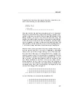
Page 48: ...he first line of the display is the groups line The groups line determines how the pins of the Vector Output I O Module are to be grouped together All 40 pins on the module must be listed in this group This line may be changed to group together the 40 pins using the following syntax GROUPS label group where GROUPS is the name of the line label is an optional label made of any ASCII characters exce...

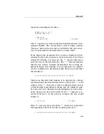
Page 49: ... a maximum of forty numbers i e 40 1 All forty pins of the Vector Output I O Module must be listed For example if all the group s consisted of one num ber forty group s would be listed on the groups line The Display Line 6 6 The display line specifies whether the data shown in the data fields are displayed in binary or hexadecimal When a vector file is first created the display line is shown as DI...

Page 50: ...esignators are case insensitive The display line could be changed to read DISPLAY hex HeX BIN Comment Lines 6 7 Comment lines can be added to the vector file on any line after the groups and display line All comment lines must begin with a Comment lines must contain only comments i e no comments can be added to the end of a data field Data Fields 6 8 Data fields consist of the data that is to be s...

Page 51: ...s are used by the TL 1 vectordrive command to determine where in the vector file to begin driving vectors The line num bers must be in the range of 1 through 8192 If a number out side this range is used an error message is displayed The first data field has its number automatically supplied when a vector file is created All other line numbers must be entered by the user These numbers do not have t...

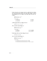
Page 52: ... DISPLAY BIN BIN and the data fields would remain the same If you did not enter a space on data field line in the previous ex ample all of the numbers in the second group would have been automatically tri stated For example if you entered 1111 the first field would have been right justified and filled in with zeroes and the second field would have been tri stated 1 00000000000000000000000000001111...

Page 53: ...y hexadecimal but is being dis played in binary For example if you wanted pin 9 to output a tri state condition in a hexadecimal data field you would enter the data line as 0100000000010000000001111111110X 1111XXXX The line on this field will continue to be displayed as a binary representation in the hexadecimal field as long as the is left in place If the character is removed the data field conve...

Page 54: ...FFFFF 0000XXXX 3 00000000 1100XX11 and the groups line was changed to read GROUPS 40 13 12 1 the vector file would change to GROUPS 40 13 12 1 DISPLAY HEX BIN TIME DATA 1 401007F 11011111XXXX 2 FFFFFFF 11110000XXXX 3 0000000 00001100XX11 If the display line was then changed to read DISPLAY BIN HEX the vector file would change to GROUPS 40 13 12 1 DISPLAY BIN HEX TIME DATA 1 01000000000100000000011...

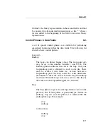
Page 55: ...ay be set to any number between 1 and 65536 The Endloop phrase indicates the end of the loop Only one loop endloop pair is allowed for each vector file There must be at least 2 data fields i e vectors between a loop endloop pair The loop count n value determines the number of times the vectors between loop and endloop are driven When the loop count n is set to 1 the effect is the same as if the lo...

Page 56: ...osing edge to assure that an input capture occurs Wait x The Wait phrase pauses vector driving until the appropriate rising or falling edge is detected on the Vector Output I O Module WAIT line before vector driving continues x may be specified as for rising edges and for falling edges x can only be set to one edge type in a vector file If more than one edge type is specified in the file an error ...

Page 57: ...01010000111 4 0000000000000000000000000000000000000000 5 1111111111111111111111111111111111111111 ENDLOOP and the vectordrive command specifies that the file begins driv ing on data field 4 the vectors are driven out in the order 4 5 2 3 4 5 2 etc ...

Page 58: ...9100A 017 6 14 ...

Page 59: ...a program to setup the output section 3 From TL 1 use a program to setup the input section 4 From TL 1 use a program to drive vectors and measure responses 5 From TL 1 use a program to process the results Section 6 Using the Vector Editor illustrated how to make vector files To make vector files that perform bus cycles see Bus Emulation Testing the IBM CGA Video Card and 68000 Bus Video Applicatio...

Page 60: ...ses arm device devname vectordrive device devname startmode now vector 1 loop until drivepoll device devname 3 ensure driving complete end loop readout device devname Process the Results for pinnum 1 to 40 alvl level device devname pin pinnum type async slvl level device devname pin pinnum type clocked cnt count device devname pin pinnum crc sig device devname pin pinnum if not expected results di...

Page 61: ...s where the individual data must be ob served a TL 1 readword function must be performed after each cycle By using the capture sync mode and placing the CAPTURE keyword in the appropriate vector in the vector file or by using the ext sync mode and connect ing the external clock line CLOCK to an address strobe or data strobe the readword function can read the stored synchronous level history This m...

Page 62: ...Output The basic test strategy for each of the main areas is defined as CRT Controller The controller to card edge interface is checked and the controller s ability to control the video in all modes is verified Video RAM The video RAM is tested by filling it with various patterns and reading back the stored information Video Character ROM Various character codes are loaded into video RAM and the p...

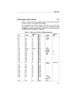
Page 63: ...tput I O Module Mapping Pin Signal Module Pin Pin Signal Module Pin A1 B1 GND A2 D0 13 B2 RESET 7 A3 D1 14 B3 5V A4 D2 15 B4 A5 D3 16 B5 A6 D4 17 B6 A7 D5 18 B7 A8 D6 19 B8 A9 D7 20 B9 12V A10 IORDY 8 WAIT B10 GND A11 AEN 5 B11 MEMW 3 A12 A19 40 B12 MEMR 4 A13 A18 39 B13 IOW 2 A14 A17 38 B14 IOR 1 A15 A16 37 B15 A16 A15 36 B16 A17 A14 35 B17 A18 A13 34 B18 A19 A12 33 B19 A20 A11 32 B20 IOCLK 6 MHz...

Page 64: ...e vectors with the bus on the Vector Output I O Module IORDY The IORDY line is connected to pin A10 of the CGA connector and pin 8 and WAIT to provide Video RAM synchronization of the Vector Output I O Module A pullup resistor is added to this line on the performance board of the Card Edge Fixture Kit 14 MHz An external signal generator provides the 14 31818 MHz signal required for Video Sync 5V 1...

Page 65: ... held for 10 ns after the falling edge of the clock WRITE DATA must be set a minimum of 165 ns before the falling edge of the E clock and held for 10 ns after the fall ing edge of the clock READ DATA must be output a maximum of 290 ns after the rising edge of the E clock and will be held for a maxi mum of 50 ns after the falling edge of the E clock Figure 7 1 MC6845 Cycle Timing Diagram The follow...

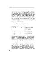
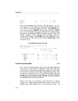
Page 66: ...D O O E E E E O O R W M M N S R C W R E D L T Y K START OF WRITE CYCLE write 3D5 data 55 1 003D5 XX 1 1 1 1 0 0 X X XXXX 2 003D5 XX 1 0 1 1 0 0 X X XXXX 3 003D5 XX 1 0 1 1 0 0 X X XXXX 4 003D5 XX 1 0 1 1 0 0 X X XXXX 5 003D5 55 1 0 1 1 0 0 X X XXXX 6 003D5 55 1 1 1 1 0 0 X X XXXX STOP Note that the grouping of vectors in the file with a few comments can be self documenting By using the appropriate...

Page 67: ...me of the RAM is much greater than that of the CRT Controller and because the RAM is shared between the controller and bus accesses the IORDY line is used with the WAIT line of the module to provide synchronization In the Video RAM Write Cycle Vector File that follows vector 1 sets addresses A19 through A0 and data D7 through D0 Vector 2 holds the address and data while MEMW goes low Upon receipt ...

Page 68: ...A19 A0 D7 D0 I I M M A R I I UNUSED O O E E E E O O R W M M N S R C W R E D L T Y K READ CYCLE address B8000 1 B8000 XX 1 1 1 1 0 0 X X XXXX 2 B8000 XX 1 1 1 0 0 0 X X XXXX WAIT 3 B8000 XX 1 1 1 0 0 0 X X XXXX CAPTURE 4 B8000 XX 1 1 1 1 0 0 X X XXXX STOP Vector File Generation 7 9 Once the basic read and write cycles have been determined the vector files to control and test the CGA Card can be bui...

Page 69: ...lare get the vector start address B8000 1 B8001 4 B8002 7 vec_num addr BB000 3 1 go do the read byte_str read_cycle vec_start vec_num check for stable levels on the read no s if instr byte_str 0 then stable read byte_nun val byte_str 2 print Read str addr 16 str byte_num 16 else unstable read print Read str addr 16 Is Not Stable end if return errflg end function READ_CYCLE VEC_START This function ...

Page 70: ... ascii screen part 2 vectorload device devname file alpha_80_2 vectordrive device devname startmode now vector 1 loop until drivepoll device devname 3 end loop vectorload device devname file read_vram read_loc addr B8000 read character 1 read_loc addr B8001 read attributes read_loc addr B8002 read character 2 read_loc addr B8003 read attributes end program 68000 BUS VIDEO APPLICATION 7 11 The vide...

Page 71: ... UUT DTACK must be applied to the WAIT input on the module There are two separate signals from the video board VDTACK a one wait state DTACK from the controller and VWAIT a three wait state DTACK from the video RAM Both of these lines are connected to the inputs of a 74LS08 AND Table 7 2 Video Board to Vector Output I O Module Mapping Pin Signal Module Pin Pin Signal Module Pin 27C A11 40 7A D6 20...

Page 72: ... by address strobe AS and memory decoding PS7 FXXXX PS6 EXXXX on the 9100A main board To access either the controller or video RAM requires the same basic cycle the only difference being the controller data is D7 through D0 and is selected by PS7 while the video RAM data is D15 through D0 and is selected by PS6 Because of the similarity of the cycles to access the controller and the video RAM only...

Page 73: ...D0 must be setup 150 ns minimum before WR goes high Data D7 through D0 must be held a minimum of 5 ns after WR goes high Address bus A11 through A1 and CE have a 0 ns hold time after WR goes high CE must be high for 300 ns between chip accesses Using an internal clock frequency of 5 MHz which gives 200 ns per vector resolution the following 2674 Video Display Controller Write Cycle vector file can...

Page 74: ...ontained under the control section of the vector file The first vector in this file sets the address Vector 2 which is driven 200 ns later holds the address sets the data sets R W and LDS low to get WR low and sets PS7 low to get CE low The WAIT statement ensures that VDTACK is returned before continuing The final vector which is driven 200 ns later holds the address and data while the CTRL signal...

Page 75: ...ddr fxxxx PS7 data LDS 1 011 XX XX 1 1 1 1 1 1 X X XXXX 2 011 XX XX 1 1 0 0 1 1 X X XXXX WAIT 3 003 XX XX 1 1 1 1 1 1 X X XXXX CAPTURE STOP The first vector in this file sets the address Vector 2 which is driven 200 ns later holds the address holds R W high and sets LDS low to get RD low and sets PS7 low to get CE low The WAIT statement ensures that VDTACK is returned before continuing The final v...

Page 76: ...e module by dedicating one of the output lines of the module to control an exclusive OR gate to be used as a programmable inverter The vector file entries for the dedicated line determine if the event connected to the other input of the gate should be inverted or not inverted before going to the WAIT input of the module In some applications WAIT may need to be checked for a level rather than an ed...

Page 77: ...sfied Figure 7 4 Using WAIT to Check for a Level Method 2 TIMING SETS 7 18 The Vector Output I O Module does not require the use of timing sets for most applications because of its pattern depth of 8192 vectors and loading time of 3 seconds for an 8K vector file However to reduce programming time or the number of vector files necessary two Vector Output I O Modules can be used to provide timing se...

Page 78: ...he address and data vectors as shown in Figure 7 5 Figure 7 5 Connecting Two Modules for Timing Sets The second module would contain the vector patterns to be out put on the address and data bus lines The number of entries in this vector file should be the same as the LOOP value set in the first module s vector file The following example demonstrates this method ...

Page 79: ...03 00 XXXX 5 01 04 13 XXXX STOP In this example module 1 is set to the appropriate syncoutput mode module 2 is set to syncoutput mode drclk and the edgeoutput clock argument is set to When module 1 begins driving out vectors its pin 32 ADDCLK line clocks the second module to get the correct address and data Each time the loop is driven module 2 gets clocked to update its address and data Note that...

Page 80: ...N S R C W R E D L T Y K START OF WRITE CYCLE write B8000 data 4107 1 B8000 41 1 1 1 1 0 0 X X XXXX 2 B8000 41 1 1 0 1 0 0 X X XXXX WAIT 3 B8000 XX 1 1 1 1 0 0 X X XXXX 4 B8001 07 1 1 1 1 0 0 X X XXXX 5 B8001 07 1 1 0 1 0 0 X X XXXX WAIT 6 B8001 XX 1 1 1 1 0 0 X X XXXX Note that the previous vector file contains writes at two different addresses The build program automatically handles the address i...

Page 81: ...ibute character input on in_text using nl addr_val_str attr_str patt_str print on t2o 1B 3 1f 1B KWrite At addr_val_str Data patt_str headinq comment for each cycle write_it 1 mid writecyc 9 1 29 addr_val_str data patt_str attr_str pick apart old cycle slip in new stuff preamble mid writecyc 10 1 7 addr_val_str patt_str write cycle to character location write_it 2 preamble mid writecyc 10 32 36 wr...

Page 82: ... t2u old_file if filestat file old_file then in_text open device old_file as input get file name of the file to store text file to print on t2o 1B 1 1f 1B JInput Name Of Output File input on t2u new_file out_text open device new_file as output Print out header information This includes the GROUPS line DISPLAY line and comments describinq signal names of the groups for n 1 to 8 print on out_text wr...

Page 83: ...A 1 Appendix A New TL 1 Commands ...

Page 84: ...9100A 017 A 2 ...

Page 85: ...yntax Diagram Description Sets the internal vector output drive clock frequency to 1 MHz 5 MHz 10 MHz or 20 MHz This command is used with the Vector Output I O Module only Arguments device list I O module name clip name or combination of these Default mod1 freq freq of 1MHz 5MHz 10MHz or 20MHz Default 1MHz ...

Page 86: ...uency of mod1 to 10MHz clockfreq mod1 10MHz Remarks The clockfreq command sets the internal clock frequency that is used to drive out vectors The frequency changes immediately upon command execution Note that there is no synchronization between the internal clocks of each I O module Changing the internal clock frequency dur ing vector driving is not recommended This frequency is also available on ...

Page 87: ...clockfreq 3 For More Information The Overview Of TL 1 section of the Programmer s Manual ...

Page 88: ...clockfreq 4 ...

Page 89: ...le only Arguments Returns Vector drive status is indicated by bit 0 Bit 0 is 0 if vector driving is not complete and is 1 if vector driving is complete Handshake status is indicated by bit 1 Bit 1 is 0 if vector driving is suspended and the selected edge of the signal on the WAIT input has not yet been received Bit 1 is 1 if the module is not awaiting a WAIT input device list I O module name clip ...

Page 90: ... vec1 edgeoutput device mod1 start at_vectordrive vectordrive device mod1 n 0 loop while n 3 n drivepoll device mod1 if n 0 then give edge to mod1 writepin device mod2 pin 1 level 1 writepin device mod2 pin 1 level 0 end if end loop Remarks If the sysncoutput mode is set to drclk or intfreq and a signal on the external STOP line is received with the proper edge vectordriving will be terminated but...

Page 91: ...drivepoll 3 For More Information The Overview Of TL 1 section of the Programmer s Manual ...

Page 92: ...drivepoll 4 ...

Page 93: ...escription Specifies the active edge for the external START STOP and DR CLK inputs used to drive out vectors Does not affect the input section hardware This command is used with the Vector Output I O Module only Arguments device list I O module name clip name or combination of these Default mod1 start edge External start edge or at_vectordrive Default stop edge External stop edge or Default ...

Page 94: ...eipt of a qualified clock This occurs regardless of the start mode argument set in the vectordrive command The start edge and the stop edge arguments have no effect on syncoutput modes pod and int The clock edge argument has no effect on syncoutput modes pod int and intfreq Related Commands syncoutput vectordrive For More Information The Overview Of TL 1 section of the Programmer s Manual clock ed...

Page 95: ... the external ENABLE line used to qualify the clocks for vector driving Does not affect the input section hardware This command is used with the Vector Output I O Module only Arguments Example 1 mod mod1 enableoutput device mod mode high device list I O module name clip module name or combination of these Default mod1 mode Enable modes always high or low Default always ...

Page 96: ...o drive out vectors If the high or low mode is selected the appropriate level must be present on the external ENABLE line to qualify the clock This command only qualifies the clock when the syncoutput mode is drclk or intfreq Both syncoutput modes int and pod clocks are always qualified Related Commands edgeoutput syncoutput vectordrive For More Information The Overview Of TL 1 section of the Prog...

Page 97: ...utclock command continues to drive vectors until the end of the vector file is reached This command is used with the Vector Output I O Module only Arguments Example 1 mod mod1 syncoutput device mod mode int syncoutput must be set to int or error occurs on strobeoutclock edgeoutput device mod start at_vectordrive vectorload device mod file vec1 vectordrive device mod arm device mod strobeoutclock d...

Page 98: ...ice mod strobeoutclock device mod if read addr 90000 55 then print Port 2 Failed 55 Clock out vector 2 AA strobeoutclock device mod if read addr 90000 AA then print Port 2 Failed AA Remarks The syncoutput mode must be int or an error is issued upon strobeoutclock execution The strobeoutclock command is useful for single step debugging It is also useful for controlling vector driving when other TL ...

Page 99: ...section hardware The actual clock selection does not occur until the vectordrive command has been executed This command is used with the Vector Output I O Module only Arguments Example 1 syncoutput device mod1 mode intfreq clockfreq device mod1 freq 10MHz vectordrive device mod1 device list I O module name clip module name or any combination of these Default mod1 sync mode Sync Modes pod drclk int...

Page 100: ...pod data or an other pod sync mode as the clock source When the syncoutput mode is set to intfreq use the clockfreq command to control the frequency of the clock When the syncoutput mode is set to int use the strobeoutclock command to clock out the vectors Related Commands clockfreq edgeoutput enableoutput strobeoutclock sync vectordrive For More Information The Overview Of TL 1 section of the Pro...

Page 101: ...cription The execution of this command enables the loaded vector file to be driven starting at the indicated vector This command is analogous to an arm command for the output This command is used with the Vector Output I O Module only Arguments device list I O module name or any combination of I O module names Default mod1 startmode Start Mode at_arm or now Default now ...

Page 102: ...tput mode is int vector driving occurs on the execution of the strobeoutput command and syncoutput mode is either drclk or intfreq and edgeoutput start is at_vectordrive vector driving occurs upon the receipt of a qualified clock and edgeoutput start is or vector driving occurs upon on first qualified clock following the receipt of the external START vector Vector number from which to begin drivin...

Page 103: ...ming of the vector driving and the response gathering hardware Once loaded a vector file can be driven repeatedly starting at any specified vector until overwritten by a writepin or writeword command Related Commands edgeoutput enableoutput syncoutput strobeoutclock vectorload For More Information The Overview Of TL 1 section of the Programmer s Manual ...

Page 104: ...vectordrive 4 ...

Page 105: ...gle vector file cannot cover more than one I O Module However vectorload may load the same file into several modules at the same time This command is used with the Vector Output I O Module only Arguments Example 1 vectorload device mod1 file hdr tmp vec1 vectordrive device mod1 device list I O module name or any combination of I O module names Default mod1 file name Absolute or relative file name ...

Page 106: ...ween an arm and a readout with no adverse effects as long as no qualified clocks are received This method works well when the input section hardware s sync mode is pod int or capture More care must be taken if the sync mode is ext When executed the vectorload command uses available memory to transfer the vector file from disk to the I O Module If the entire file fits into memory only one disk acce...

Page 107: ...vectorload 3 For More Information The Overview Of TL 1 section of the Programmer s Manual ...

Page 108: ...vectorload 4 ...

Page 109: ...talled on A side Clip I O Mod Pin Clip I O Mod Pin 1 1 14 20 2 2 13 19 3 3 12 18 4 4 11 17 5 5 10 16 6 6 9 15 7 7 8 14 Clip size 14 module installed on B side Clip I O Mod Pin Clip I O Mod Pin 1 21 14 40 2 22 13 39 3 23 12 38 4 24 11 37 5 25 10 36 6 26 9 35 7 27 8 34 ...

Page 110: ...Mod Pin Clip I O Mod Pin 1 1 16 20 2 2 15 19 3 3 14 18 4 4 13 17 5 5 12 16 6 6 11 15 7 7 10 14 8 8 9 13 Clip size 16 module installed on B side Clip I O Mod Pin Clip I O Mod Pin 1 21 16 40 2 22 15 39 3 23 14 38 4 24 13 37 5 25 12 36 6 26 11 35 7 27 10 34 8 28 9 33 ...

Page 111: ...p I O Mod Pin 1 1 18 20 2 2 17 19 3 3 16 18 4 4 15 17 5 5 14 16 6 6 13 15 7 7 12 14 8 8 11 13 9 9 10 12 Clip size 18 module installed on B side Clip I O Mod Pin Clip I O Mod Pin 1 21 18 40 2 22 17 39 3 23 16 38 4 24 15 37 5 25 14 36 6 26 13 35 7 27 12 34 8 28 11 33 9 29 10 32 ...

Page 112: ...n 1 1 20 20 2 2 19 19 3 3 18 18 4 4 17 17 5 5 16 16 6 6 15 15 7 7 14 14 8 8 13 13 9 9 12 12 10 10 11 11 Clip size 20 module installed on B side Clip I O Mod Pin Clip I O Mod Pin 1 21 20 40 2 22 19 39 3 23 18 38 4 24 17 37 5 25 16 36 6 26 15 35 7 27 14 34 8 28 13 33 9 29 12 32 10 30 11 31 ...

Page 113: ...3 22 18 4 4 21 17 5 5 20 16 6 6 19 15 7 7 18 14 8 8 17 13 9 9 16 12 10 10 15 11 11 29 14 32 12 30 13 31 Clip size 24 module installed on B side Clip I O Mod Pin Clip I O Mod Pin 1 21 24 40 2 22 23 39 3 23 22 38 4 24 21 37 5 25 20 36 6 26 19 35 7 27 18 34 8 28 17 33 9 29 16 32 10 30 15 31 11 9 14 12 12 10 13 11 ...

Page 114: ...3 9 9 20 32 10 10 19 31 11 11 18 30 12 12 17 29 13 13 16 28 14 14 15 27 Clip size 40 Clip I O Mod Pin Clip I O Mod Pin 1 1 40 40 2 2 39 39 3 3 38 38 4 4 37 37 5 5 36 36 6 6 35 35 7 7 34 34 8 8 33 33 9 9 32 32 10 10 31 31 11 11 30 30 12 12 29 29 13 13 28 28 14 14 27 27 15 15 26 26 16 16 25 25 17 17 24 24 18 18 23 23 19 19 22 22 20 20 21 21 ...

Page 115: ...pendix C Keypad Reference Changes This appendix lists the changes made to the keypad reference syntax to accommodate the 9100A 017 Vector Output I O Module Only the MAIN MENU key and the SYNC key are changed ...

Page 116: ...9100A 017 C 2 ...

Page 117: ...9100A 017 C 3 ...

Page 118: ...9100A 017 C 4 ...

Page 119: ...ture kit 4 10 Card edge interface module 4 10 CGA Mapping 7 5 CGA Program Example 7 11 CGA Video Card 7 4 Changing the WAIT edge 7 18 Clip modules 4 1 4 9 CLOCK 4 1 Clock selection 3 1 Clocked level history register 4 12 clockfreq 3 1 5 1 Appendix A Comment lines 6 6 COMMON 4 1 4 3 compare 4 3 Completion status 3 5 Connecting the module to the mainframe 4 5 Connecting the module to the UUT 4 9 Con...

Page 120: ...t 5 3 Appendix A Endloop 6 11 External I O Module to 4 7 External lines 4 10 External sync mode 4 11 Fixture 4 10 7 5 7 13 Flying lead set 4 10 Freerun sync mode 4 14 Fuse 4 3 Groups line 6 4 Handshake input 4 2 Handshake status Appendix A Handshaking 3 2 I O Module to external 4 7 I O Module clip pin mapping Appendix B I O Module to pod 4 8 INT CLK 4 3 4 16 7 3 Internal clock delay 4 7 Internal s...

Page 121: ...ipping temperature 2 4 strobeoutclock 5 3 Appendix A sync 4 13 4 14 Synchronized data gathering 3 2 Synchronizing multiple module vectors 4 16 Synchronizing the module to the UUT 4 11 Synchronizing the UUT 3 1 Synchronizing the Vector Output I O Module 3 1 syncoutput 3 1 5 3 7 21 Appendix A Testing the video board 7 12 TL 1 commands Appendix A TL 1 vector file generation 7 21 Timing sets 7 19 Tran...

Page 122: ... clock source Appendix A Vector output operation 3 1 vectordrive 5 3 6 7 6 12 Appendix A vectorload 5 3 Appendix A Video RAM bus cycles 7 9 WAIT 3 2 4 2 5 1 6 12 WAIT application 7 18 Working with the vector file 6 4 writepin 3 2 5 3 writeword 3 2 5 3 ...

Reviews: